TI-UC1854.pdf
需积分: 9 177 浏览量
2022-10-26
23:44:27
上传
评论 5
收藏 1.78MB PDF 举报

+
–
16
3
4
ISENSE
5
2
PKLMT
14
13
12 1
9
VREF
VREF
VREF
RSETSSCT
15
VCC
VCC
11
7
VSENSE
8
6
10
VREF
VCC
ENA
IAC
VRMS
EMI
Filter
Line
Input
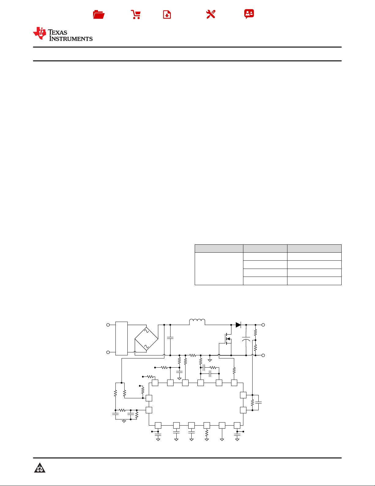
UC3854
VOUT
400 VDC
MULTOUT CAOUT
GTDRV
VAOUT
GND
Copyright © 2016, Texas Instruments Incorporated
Product
Folder
Order
Now
Technical
Documents
Tools &
Software
Support &
Community
An IMPORTANT NOTICE at the end of this data sheet addresses availability, warranty, changes, use in safety-critical applications,
intellectual property matters and other important disclaimers. PRODUCTION DATA.
UC1854
,
UC2854
,
UC3854
SLUS336A –JUNE 1998–REVISED DECEMBER 2016
UCx854 High-Power Factor Preregulator
1
1 Features
1
• Control Boost PWM to 0.99 Power Factor
• Limit Line-Current Distortion to < 5%
• World-Wide Operation Without Switches
• Feedforward Line Regulation
• Average Current-Mode Control
• Low Noise Sensitivity
• Low Startup Supply Current
• Fixed-Frequency PWM Drive
• Low-Offset Analog Multiplier and Divider
• 1-A Totem-Pole Gate Driver
• Precision Voltage Reference
2 Applications
• Offline AC-to-DC Converters
• Medical, Industrial, Telecom, and IT Power
Supplies
• Uninterruptible Power Supplies (UPS)
• Appliances and White Goods
3 Description
The UC1854 provides active-power factor correction
for power systems that otherwise would draw non-
sinusoidal current from sinusoidal power lines. This
device implements all the control functions necessary
to build a power supply capable of optimally using
available power-line current while minimizing line-
current distortion. To do this, the UC1854 contains a
voltage amplifier, an analog multiplier and divider, a
current amplifier, and a fixed-frequency PWM.
In addition, the UC1854 contains a power MOSFET-
compatible gate driver, 7.5-V reference, line
anticipator, load-enable comparator, low-supply
detector, and overcurrent comparator.
The UC1854 uses average current-mode control to
accomplish fixed-frequency current control with
stability and low distortion. Unlike peak current-mode,
average current control accurately maintains
sinusoidal line current without slope compensation
and with minimal response to noise transients.
The high reference voltage and high oscillator
amplitude of the UC1854 minimize noise sensitivity
while fast PWM elements permit chopping
frequencies above 200 kHz. The UC1854 is used in
single-phase and three-phase systems with line
voltages that vary from 75 V to 275 V and line
frequencies across the 50-Hz to 400-Hz range. To
reduce the burden on the circuitry that supplies power
to this device, the UC1854 features low starting
supply current.
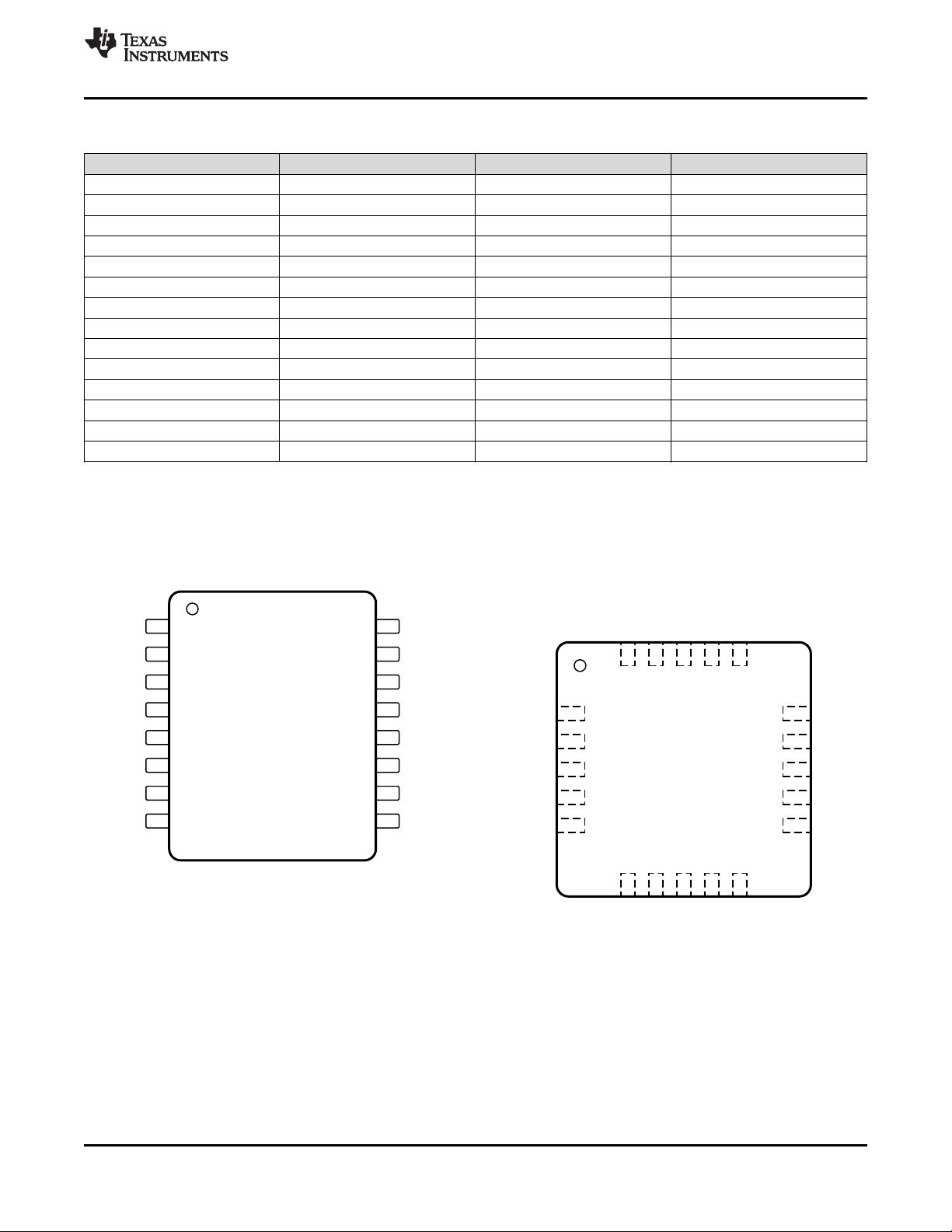
These devices are available packaged in 16-pin
plastic and ceramic dual in-line packages, and a
variety of surface-mount packages.
Device Information
(1)
PART NUMBER PACKAGE BODY SIZE (NOM)
UC1854, UC2854,
UC3854
SOIC (16) 7.50 mm × 10.30 mm
PLCC (20) 8.96 mm × 8.96 mm
CDIP (16) 6.92 mm × 19.56 mm
PDIP (16) 6.35 mm × 19.30 mm
(1) For all available packages, see the orderable addendum at
the end of the data sheet.
Block Diagram


剩余29页未读,继续阅读
资源评论


