没有合适的资源?快使用搜索试试~ 我知道了~
TI-UC2907.pdf
需积分: 9 0 下载量 196 浏览量
2022-10-28
21:07:45
上传
评论 5
收藏 788KB PDF 举报
温馨提示
试读
12页
TI-UC2907.pdf
资源详情
资源评论
资源推荐
SLUS165C – MARCH 1999 - REVISED JANUARY 2002
1
www.ti.com
FEATURES
D
Fully Differential High Impedance Voltage
Sensing
D Accurate Current Amplifier for Precise
Current Sharing
D Opto Coupler Driving Capability
D 1.25% Trimmed Reference
D Master Status Indication
D 4.5-V to 35-V Operation
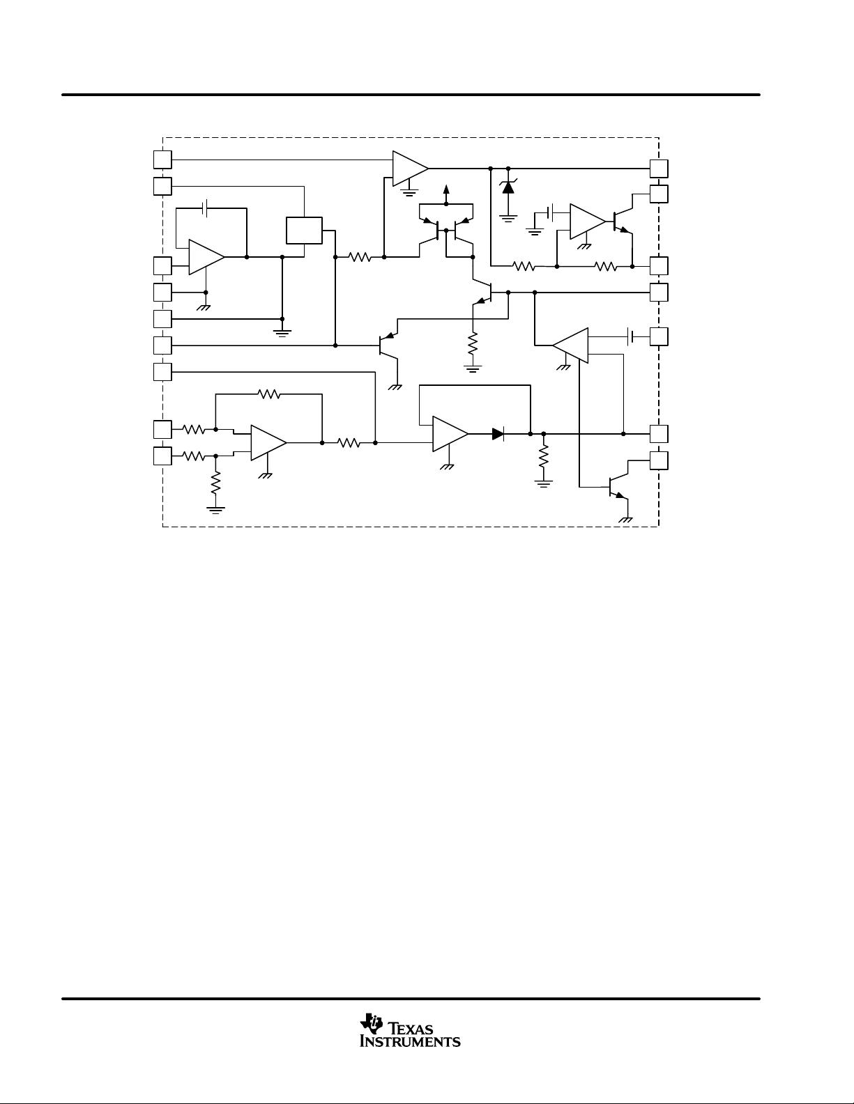
DESCRIPTION
The UCx907 family of load share controller ICs provides all the necessary features to allow
multiple-independent-power modules to be paralleled such that each module supplies only its proportionate share
to total-load current.
This sharing is accomplished by controlling each module’s power stage with a command generated from a
voltage-feedback amplifier whose reference can be independently adjusted in response to a common-share-bus
voltage. By monitoring the current from each module, the current share bus circuitry determines which paralleled
module would normally have the highest output current and, with the designation of this unit as the master, adjusts
all the other modules to increase their output current to within 2.5% of that of the master.
The current share bus signal interconnecting all the paralleled modules is a low-impedance, noise-insensitive line
which will not interfere with allowing each module to act independently should the bus become open or shorted to
ground. The UC3907 controller will reside on the output side of each power module and its overall function is to supply
a voltage feedback loop. The specific architecture of the power stage is unimportant. Either switching or linear designs
may be utilized and the control signal may be either directly coupled or isolated though the use of an optocoupler or
other isolated medium.
Other features of the UC3907 include 1.25% accurate reference: a low-loss, fixed-gain current-sense amplifier, a fully
differential, high-impedance voltage sensing capability, and a status indicator to designate which module is
performing as master.
Copyright 2000, Texas Instruments Incorporated
Please be aware that an important notice concerning availability, standard warranty, and use in critical applications of
Texas Instruments semiconductor products and disclaimers thereto appears at the end of this data sheet.
1
2
3
4
5
6
7
8
16
15
14
13
12
11
10
9
C/S OUT
C/S (+)
C/S (–)
(–) SENSE
POWER RETURN
ARTIFICIAL GND
VREF
ISET
STATUS INDICATE
CURRENT SHARE BUS
ADJ OUT
ADJ INPUT
COMP
(+) SENSE
VCC
OPTO DRIVE
DIL-16 J or N PACKAGE
(TOP VIEW)
1
2
3
4
5
6
7
8
16
15
14
13
12
11
10
9
C/S OUT
C/S (+)
C/S (–)
(–) SENSE
POWER RETURN
ARTIFICIAL GND
VREF
ISET
STATUS INDICATE
CURRENT SHARE BUS
ADJ OUT
ADJ INPUT
COMP
(+) SENSE
VCC
OPTO DRIVE
SOIC-16 DW PACKAGE
(TOP VIEW)
1920132
17
18
16
15
14
1312119 10
5
4
6
7
8
ADJ OUT
ADJ INPUT
N/C
COMP
(+) SENSE
C/S (–)
(–) SENSE
N/C
POWER RETURN
ARTIFICIAL GND
C/S (+)
C/S OUT
N/C
STATUS INDICATE
CURRENT SHARE BUS
ISET
N/C
OPTO DRIVE
VCC
VREF
PLCC-20, LCC-20,
Q OR L PACKAGE
(TOP VIEW)
SLUS165C – MARCH 1999 - REVISED JANUARY 2002
2
www.ti.com
block diagram
11
14
10
13
8
9
12
15
16
7
5
4
1
6
3
2
2 k
Ω
2 k
Ω
+
–
40 k
Ω
40 k
Ω
CURRENT SENSE
AMPLIFIER
100
+
–
BUFFER
AMPLIFIER
+
–
+
50 mV
ADJUST
AMPLIFIER
ADJ
V
CC
1 k
Ω
V
REF
1.75 V
+
–
+
GROUND
AMPLIFIER
0.25 V
GND
+
–
50 k
Ω
20 k
Ω
+
1.0 V
1.75 V
VOLTAGE ERROR AMPLIFIER
STATUS INDICATE
CURRENT SHARE BUS
ADJ INPUT
ADJ OUT
ISET
OPTO DRIVE
COMP
(+) SENSE
VCC (4.5 V TO 35 V)
(–) SENSE
POWER RTN
ARTIFICIAL GND
VREF
C/S OUT
C/S (–)
C/S (+)
DRIVE
AMPLIFIER
+
–
DRV
10 k
Ω
17.5 k
Ω
absolute maximum ratings over operating free-air temperature (unless otherwise noted)
†
Supply voltage 35 V. . . . . . . . . . . . . . . . . . . . . . . . . . . . . . . . . . . . . . . . . . . . . . . . . . . . . . . . . . . . . . . . . . . . . . . . . . . . .
Opto out voltage 35 V. . . . . . . . . . . . . . . . . . . . . . . . . . . . . . . . . . . . . . . . . . . . . . . . . . . . . . . . . . . . . . . . . . . . . . . . . . .
Opto out current 20 mA. . . . . . . . . . . . . . . . . . . . . . . . . . . . . . . . . . . . . . . . . . . . . . . . . . . . . . . . . . . . . . . . . . . . . . . . . . .
Status indicate sink current 20 mA. . . . . . . . . . . . . . . . . . . . . . . . . . . . . . . . . . . . . . . . . . . . . . . . . . . . . . . . . . . . . . . . .
C/S input voltage 35 V. . . . . . . . . . . . . . . . . . . . . . . . . . . . . . . . . . . . . . . . . . . . . . . . . . . . . . . . . . . . . . . . . . . . . . . . . . .
Share bus voltage –0.3 V to 35 V. . . . . . . . . . . . . . . . . . . . . . . . . . . . . . . . . . . . . . . . . . . . . . . . . . . . . . . . . . . . . . . . . .
Other analog inputs and outputs (zener clamped) maximum forced voltage –0.3 V to10 V. . . . . . . . . . . . . . . .
Other analog inputs and outputs (zener clamped) maximum forced current ±10 mA. . . . . . . . . . . . . . . . . . . . .
Ground amp sink current 50 mA. . . . . . . . . . . . . . . . . . . . . . . . . . . . . . . . . . . . . . . . . . . . . . . . . . . . . . . . . . . . . . . . . . .
Pins 1, 9, 12, 15 sink current 20 mA. . . . . . . . . . . . . . . . . . . . . . . . . . . . . . . . . . . . . . . . . . . . . . . . . . . . . . . . . . . . . . . .
Storage temperature range, T
stg
–65°C to 150°C. . . . . . . . . . . . . . . . . . . . . . . . . . . . . . . . . . . . . . . . . . . . . . . . . . .
Junction temperature, T
J
–55°C to 150°C. . . . . . . . . . . . . . . . . . . . . . . . . . . . . . . . . . . . . . . . . . . . . . . . . . . . . . . . . .
Lead temperature (solder 10 seconds) 300°C. . . . . . . . . . . . . . . . . . . . . . . . . . . . . . . . . . . . . . . . . . . . . . . . . . . . . . .
†
Pin Nos. refer to 16 Pin DIL Package.
‡
Currents are positive into, negative out of the specified terminal. Consult packaging section of databook for thermal limitations and considerations
of package.
SLUS165C – MARCH 1999 - REVISED JANUARY 2002
3
www.ti.com
electrical characteristics, these specifications apply for T
A
= –55°C to 125°C for UC1907, –40°C to
85°C for UC2907, and 0°C to 70°C for UC3907, V
IN
= 15 V, T
A
= T
J
(unless otherwise stated )
PARAMETER TEST CONDITIONS MIN TYP MAX UNITS
Voltage Amp Section
Inp t oltage
COMP = 1 V, T
A
= 25°C 1.975 2.000 2.025 V
Input voltage
COMP = 1 V, over temp 1.960 2.000 2.040 V
Line regulation V
IN
= 4.5 V to 35 V 15 mV
Load regulation I
L
reference = 0.0 mA to –10 mA 10 mV
Long term stability T
A
= 125°C, 1000hrs See Note 2 5 25 mV
Total output variation Line, load, temp 1.960 2.040
Input adjust range ADJ OUT from max high to max low 85 100 115 mV
Input bias current –1 µA
Open loop gain COMP = 0.75 V to 1.5 V 65 dB
Unity gain bandwidth T
A
= 25°C See Note 2 700 kHz
Output sink current (+) SENSE = 2.2 V, COMP = 1 V 6 15 mA
Output source current (+) SENSE = 1.8 V, COMP = 1 V 400 600 µA
V
OUT
high (+) SENSE = 1.8 V, I
L
= –400 µΑ 1.85 2 V
V
OUT
low (+) SENSE = 2.2 V, I
L
= 1 mA 0.15 0.40 V
Reference Section
O tp t oltage
T
A
= 25°C 1.970 2.000 2.030 V
Output voltage
Over operating temp 1.955 2.000 2.045 V
Short circuit current VREF = 0.0 V –15 –30 –60 mA
Ground Amp Section
Output voltage 200 250 300 mV
Common mode variation (–) SENSE from 0.0 V to 2 V 5 mV
Load reg lation
I
L
= 0.0 mA to 20 mA, T
A
= 25°C 10 mV
Load regulation
I
L
= 0.0 mA to 20 mA, over temp 15 mV
Adjust Amp Section
Input offset voltage ADJ OUT = 1.5 V, V
CM
= 0.0 V 40 50 60 mV
Input bias current –2 µA
Open loop gain 1.5 V ≤ ADJ OUT ≤ 2.25 V 65 dB
Unity gain bandwidth T
A
= 25°C, C
OUT
=1 µF See Note 2 500 Hz
Transconductance I
OUT
= –10 µA to 10 µA, V
OUT
= 1.5 V 1.7 3 4.5 ms
Output sink current V
ID
= 0.0 V, ADJ OUT = 1.5 V 55 135 225 µA
Output source current V
ID
= 250 mV, ADJ OUT = 1.5 V 110 200 350 µA
V
OUT
high V
ID
= 250 mV, I
OUT
= – 50 mA 2.20 2.70 2.90 V
V
OUT
low V
ID
= 0.0 V, I
OUT
= 50 mA 0.75 1.15 V
Common mode rejection ratio V
CM
= 0.0 to 10 V 70 dB
Output gain to V/A
V
OUT
ADJ OUT = 1.5 V to 2 V,
∆(+) SENSE/ ∆ADJ OUT
50 57 64 mV/V
NOTE 1: Unless otherwise specified all voltages are with respect to (–) SENSE. Currents are positive into, negative out of the specified terminal.
NOTE 2: Ensured by design. Not production tested.
剩余11页未读,继续阅读
不觉明了
- 粉丝: 3164
- 资源: 5419
上传资源 快速赚钱
- 我的内容管理 展开
- 我的资源 快来上传第一个资源
- 我的收益 登录查看自己的收益
- 我的积分 登录查看自己的积分
- 我的C币 登录后查看C币余额
- 我的收藏
- 我的下载
- 下载帮助
安全验证
文档复制为VIP权益,开通VIP直接复制
信息提交成功
评论0