TI-UC3914.pdf
需积分: 9 134 浏览量
2022-11-15
23:45:58
上传
评论 5
收藏 1.07MB PDF 举报

SLUS425C − DECEMBER 2003 − REVISED JULY 2004
1
www.ti.com
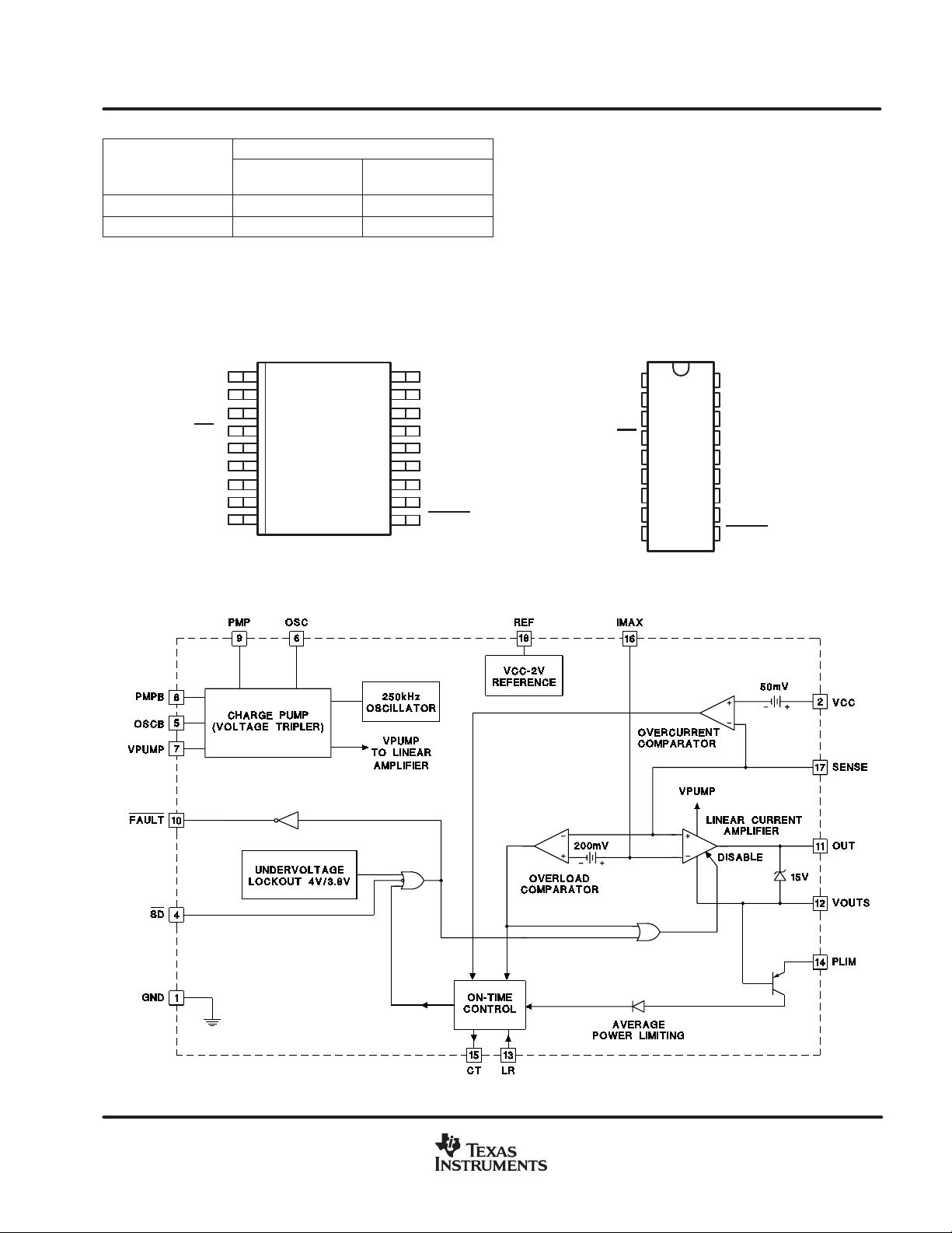
FEATURES
D
5-V to 35-V Operation
D Precision Maximum Current Control
D Precision Fault Threshold
D Programmable Average Power Limiting
D Programmable Overcurrent Limit
D Shutdown Control
D Charge Pump for Low R
DS(on)
High-Side
Drive
D Latch Reset Function Available
D Output Drive V
GS
Clamping
D Fault Output Indication
D 18-Pin DIL and SOIC Packages
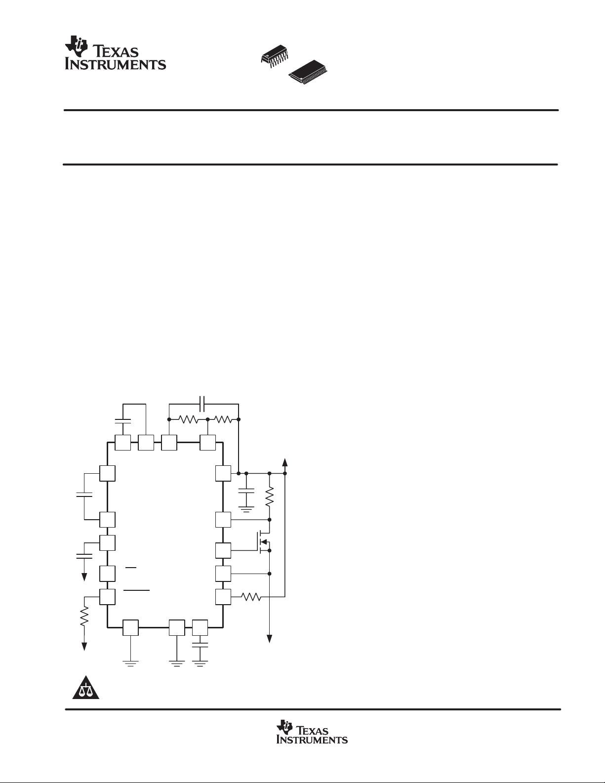
SIMPLIFIED APPLICATION DIAGRAM
DESCRIPTION
The UC3914 family of hot swap power managers
provides complete power management, hot swap
and fault handling capability. Integrating this part
and a few external components, allows a board to
be swapped in or out upon failure or system
modification without removing power to the
hardware, while maintaining the integrity of the
powered system. Complementary output drivers
and diodes have been integrated for use with
external capacitors as a charge pump to ensure
sufficient gate drive to the external N-channel
MOSFET transistor for low R
DS(on)
. All control and
housekeeping functions are integrated and
externally programmable and include the fault
current level, maximum output sourcing current,
maximum fault time and average power limiting of
the external FET. The UC3914 features a duty
ratio current limiting technique, which provides
peak load capability while limiting the average
power dissipation of the external pass transistor
during fault conditions. The fault level is fixed at
50 mV with respect to VCC to minimize total
dropout.
The fault current level is set with an external
current sense resistor. The maximum allowable
sourcing current is programmed by using a
resistor divider from VCC to REF to set the voltage
on IMAX. The maximum current level, when the
output appears as a current source is (V
VCC
−
V
IMAX
)/R
SENSE
.
This part is offered in both 18-pin DW wide-body
(SOIC) and dual-in-line (DIL) packages.
PRODUCT PREVIEW
!" ##$% &'(#% )$ !"*$
'$%+ &)"%$ '$*$,&!$- )""#$%# '"" "' )$
%&$##"% "$ '$%+ +",%- $."% %(!$% $%$*$% )$ +)
#)"+$ '%#($ )$%$ &'(#% /)( #$-
Copyright 2003, Texas Instruments Incorporated
Please be aware that an important notice concerning availability, standard warranty, and use in critical applications of
Texas Instruments semiconductor products and disclaimers thereto appears at the end of this data sheet.
UDG−03114
SD
FAULT
V
OUT
V
OUT
1
5
7
4
18 16
2
17
REF IMAX
VCC
SENSE
PMPB
OSCB
VPUMP
10
1
GND
11
12
14
15
OUT
VOUTS
PLIM
CT
13
LR
9
PMP
6
OSC
UC2914/UC3914
V
CC
V
CC

剩余26页未读,继续阅读


评论0
最新资源