没有合适的资源?快使用搜索试试~ 我知道了~
TI-UC1903.pdf
需积分: 10 0 下载量 91 浏览量
2022-11-16
23:02:43
上传
评论 5
收藏 862KB PDF 举报
温馨提示
试读
15页
TI-UC1903.pdf
资源推荐
资源详情
资源评论
1
FEATURES DESCRIPTION
BLOCK DIAGRAM
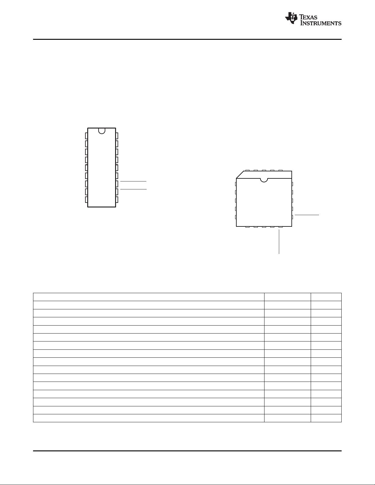
Note: Pin numbers refer to J, N and DW packages.
UC1903
UC2903
UC3903
www.ti.com
........................................................................................................................................ SLUS233A – OCTOBER 1999 – REVISED SEPTEMBER 2008
Quad Supply and Line Monitor
• Inputs for Monitoring up to Four Separate
The UC1903 family of quad supply and line monitor
Supply Voltage Levels
integrated circuits will respond to under- and
over-voltage conditions on up to four continuously
• Internal Inverter for Sensing a Negative Supply
monitored voltage levels. An internal op-amp inverter
Voltage
allows at least one of these levels to be negative. A
• Line/Switch Sense Input for Early Power
separate line/switcher sense input is available to
Source Failure Warning
provide early warning of line or other power source
• Programmable Under- and Over-Voltage Fault
failures.
Thresholds with Proportional Hysteresis
The fault window adjustment circuit on these devices
• A Precision 2.5-V Reference
provides easy programming of under- and
over-voltage thresholds. The thresholds, centered
• General Purpose Op-Amp for Auxiliary Use
around a precision 2.5-V reference, have an input
• Three High Current, >3 0mA, Open-Collector
hysteresis that scales with the window width for
Outputs Indicate Over-Voltage, Under-Voltage
precise, glitch-free operation. A reference output pin
and Power OK Conditions
allows the sense input fault windows to be scaled
• 8-V to 40-V Supply Operation with 7-mA
independently using simple resistive dividers.
Stand-By Current
The three open collector outputs on these devices
sink in excess of 30 mA of load current when active.
The under- and over-voltage outputs respond after
separate, user defined, delays to respective fault
conditions. The third output is active during any fault
condition including under- and over-voltage,
line/switcher faults, and input supply under-voltage.
The off state of this output indicates a "power OK"
situation.
1
Please be aware that an important notice concerning availability, standard warranty, and use in critical applications of Texas
Instruments semiconductor products and disclaimers thereto appears at the end of this data sheet.
PRODUCTION DATA information is current as of publication date.
Copyright © 1999 – 2008, Texas Instruments Incorporated
Products conform to specifications per the terms of the Texas
Instruments standard warranty. Production processing does not
necessarily include testing of all parameters.
DESCRIPTION (CONT.)
CONNECTION DIAGRAMS
1
2
3
4
5
6
7
8
9
18
17
16
15
14
13
12
11
10
+VIN
V (2.5V)
REF
GND
WINDOW ADJUST
SENSE4
INVERT INPUT
SENSE4
G.P.OP-AMP INV.
LINE/SWITCHERSENSE
POWEROK
UVDELAY
UVFAULT
SENSE3
SENSE2
SENSE1
G.P.OP-AMP N.I.
G.P.OP-AMP OUT
OVFAULT
OVDELAY
DIL-18,SOIC-18
JorN,DWPACKAGE
(TOP VIEW)
3 2 1 20 19
18
17
16
15
14
9 11 12 1310
4
5
6
7
8
+VIN
WINDOW ADJUST
V (2.5V)
REF
GND
GND
NC
SENSE4INVERT
INPUT
SENSE4
SENSE3
SENSE2
SENSE1
OVDELA
Y
OVFAULT
UVFAULT
UVDELAY
LINE/SWITCHER
SENSE
POWEROK
G.P.OP-AMP OUT
G.P.OP-AMP N.I.
G.P.OP-AMP INV
PLCC-20,LCC-20
Q,L PACKAGE
(TOP VIEW)
ABSOLUTE MAXIMUM RATINGS
(1)
UC1903
UC2903
UC3903
SLUS233A – OCTOBER 1999 – REVISED SEPTEMBER 2008 ........................................................................................................................................
www.ti.com
An additional, uncommitted, general purpose op-amp is also included. This op-amp, capable of sourcing 20 mA
of output current, can be used for a number of auxiliary functions including the sensing and amplification of a
feedback error signal when the 2.5-V output is used as a system reference.
These parts operate over an 8-V to 40-V input supply range and require a typical stand-by current of only 7 mA.
over operating free-air temperature range (unless otherwise noted)
VALUE UNIT
+VIN Supply Voltage +40 V
Open Collector Output Voltages. +40 V
Open Collector Output Currents. 50 mA
Sense 1-4 Input Voltages – 0.3 to +20 V
Line/Switcher Sense Input Voltage – 0.3 to +40 V
Op-Amp and Inverter Input Voltages – 0.3 to +40 V
Op-Amp and Inverter Output Currents . – 40 mA
Window Adjust Voltage. 0.0 to +10 V
Delay Pin Voltages 0.0 to +5 V
Reference Output Current – 40 mA
Power Dissipation at T
A
= 25 ° C
(1)
1000 mW
Power Dissipation at T
C
= 25 ° C
(1)
2000 mW
Operating Junction Temperature – 55 to +150 ° C
Storage Temperature – 65 to +150 C
Lead Temperature (Soldering, 10 Seconds) 300 ° C
(1) Voltages are referenced to ground (Pin 3). Currents are positive into, negative out of, the specified terminals. Consult Packaging Section
of Databook for thermal limitations and considerations of package.
2 Submit Documentation Feedback Copyright © 1999 – 2008, Texas Instruments Incorporated
Product Folder Link(s): UC1903 UC2903 UC3903
ELECTRICAL CHARACTERISTICS
UC1903
UC2903
UC3903
www.ti.com
........................................................................................................................................ SLUS233A – OCTOBER 1999 – REVISED SEPTEMBER 2008
Unless otherwise stated, these specifications apply for T
A
= – 55 ° C to +125 ° C for the UC1903; – 40 ° C to +85 ° C for the
UC2903; and 0 ° C to +70 ° C for the UC3903; +V
IN
= 15V; Sense Inputs (Pins 6 – 9 and Pin 15) = 2.5V; V
PIN
4 = 1.0V, T
A
= T
J
.
UC1903 / UC2903 UC3903
PARAMETER TEST CONDITIONS UNIT
MIN TYP MAX MIN TYP MAX
SUPPLY
Input Supply Current No Faults 7 9 7 11 mA
UV, OV and Line Fault 10 15 10 18 mA
Supply Under Voltage Threshold Fault Outputs Enabled 6.0 7.0 7.5 5.5 7.0 8.0 V
(V
SUV
)
Minimum Supply to Enable Power 3.0 4.0 3.0 4.0 V
OK Output
REFERENCE
Output Voltage (V
REF
) T
J
= 25 ° C 2.485 2.5 2.515 2.470 2.5 2.530 V
Over Temperature 2.465 2.535 2.465 2.535 V
Load Regulation IL = 0 to 10mA 1 10 1 15 mV
Line Regulation +V
IN
= 8 to 40V 1 4 1 8 mV
Short Circuit Current TJ = 25 ° C 40 40 mA
FAULT THRESHOLDS
(1)
OV Threshold Adj. Offset from V
REF
as a function of V
PIN
0.230 0.25 0.270 0.230 0.25 0.270 V/V
4 Input = Low to High, 0.5V ≤ V
PIN
4 ≤ 2.5V
UV Threshold Adj. Offset from V
REF
as a function of V
PIN
– 0.270 – 0.25 – 0.230 – 0.270 – 0.25 – 0.270 V/V
4 Input = High to Low, 0.5V ≤ V
PIN
4 ≤ 2.5V
OV & UV Threshold Hyst. 0.5V ≤ V
PIN
4 ≤ 2.5V 10 20 30 10 20 30 mV/V
OV & UV Threshold Supply +V
IN
= 8V to 40V 0.002 0.01 0.002 0.02 %/V
Sensitivity
Adjust Pin (Pin 4) Input Bias Current 0.5V ≤ VP
IN
4 ≤ 2.5V ± 1 ± 10 ± 1 ± 12 µ A/V
Line Sense Threshold Input = High to Low 1.94 2.0 2.06 1.9 2.0 2.1 V
Line Sense Threshold Hyst. 125 175 225 100 175 250 mV
SENSE INPUTS
Input = 2.8V
(2)
1 3 1 6 µ A
Sense 1-4 Input Bias Current
Input = 2.2
(2)
– 1 – 3 – 1 -6 µ A
Line Sense Input Bias Current Input = 2.3V
(2)
1 3 1 6 µ A
OV AND UV FAULT DELAY
Charging Current 60 60 µ A
Threshold Voltage Delay Pin = Low to High 1.8 1.8 V
Threshold Hysteresis T
J
= 25 ° C 250 250 mV
Delay Ratio of Threshold Voltage to Charging 20 30 50 20 30 50 ms/ µ F
Current
(1) Reference to pin numbers in this specification pertain to 18 pin DIL N and J packages and 18 pin SOIC DW package.
(2) These currents represent maximum input bias currents required as the sense inputs cross appropriate thresholds.
Copyright © 1999 – 2008, Texas Instruments Incorporated Submit Documentation Feedback 3
Product Folder Link(s): UC1903 UC2903 UC3903
剩余14页未读,继续阅读
资源评论
不觉明了
- 粉丝: 3164
- 资源: 5429
上传资源 快速赚钱
- 我的内容管理 展开
- 我的资源 快来上传第一个资源
- 我的收益 登录查看自己的收益
- 我的积分 登录查看自己的积分
- 我的C币 登录后查看C币余额
- 我的收藏
- 我的下载
- 下载帮助
安全验证
文档复制为VIP权益,开通VIP直接复制
信息提交成功