没有合适的资源?快使用搜索试试~ 我知道了~
TI-UC2879.pdf
需积分: 5 0 下载量 157 浏览量
2022-10-28
21:04:01
上传
评论 5
收藏 1.2MB PDF 举报
温馨提示
试读
17页
TI-UC2879.pdf
资源详情
资源评论
资源推荐
www.ti.com
FEATURES DESCRIPTION
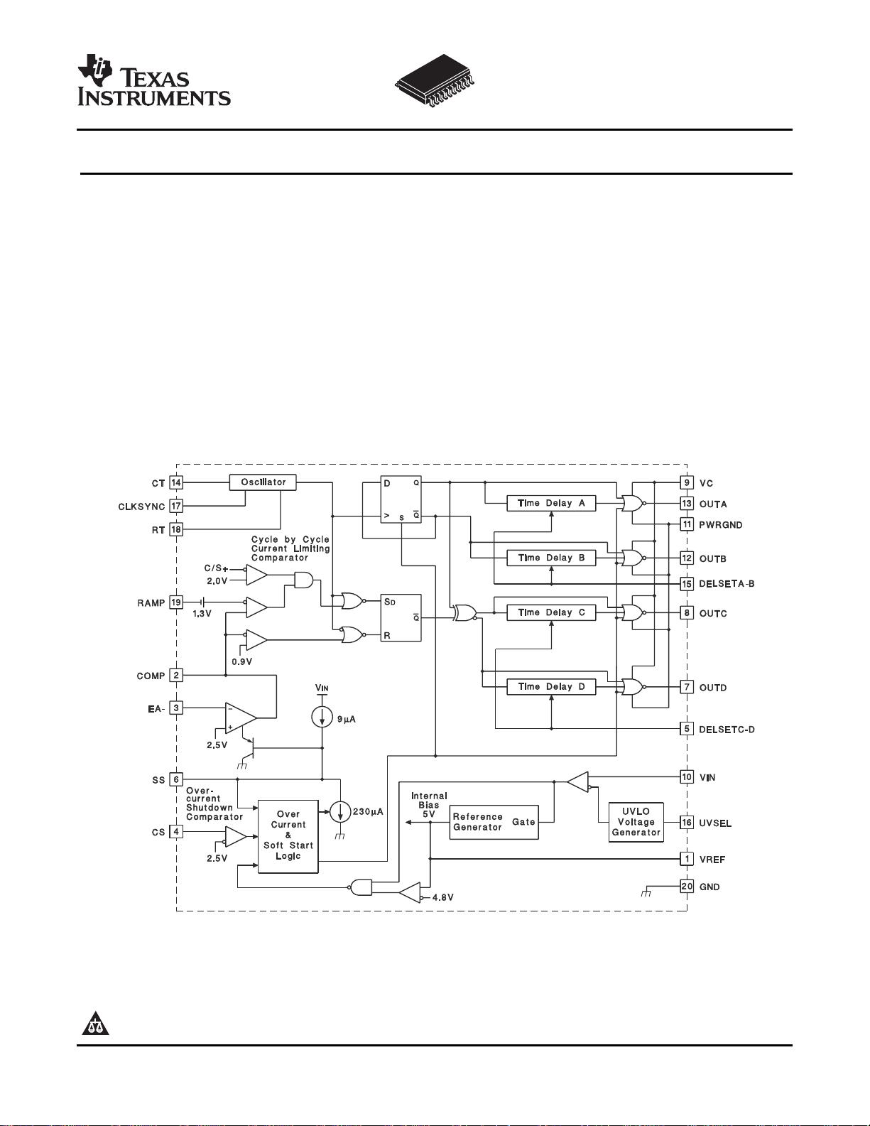
BLOCK DIAGRAM
UC1879
UC2879
UC3879
SLUS230B – JUNE 1998 – REVISED JUNE 2007
PHASE SHIFT RESONANT CONTROLLER
• Programmable Output Turn On Delay; Zero
The UC3879 controls a bridge power stage by phase
Delay Available
shifting the switching of one half-bridge with respect
to the other. This allows constant frequency pulse
• Compatible with Voltage Mode or Current
width modulation in combination with resonant,
Mode Topologies
zero-voltage switching for high efficiency
• Practical Operation at Switching Frequencies
performance. The UC3879 can be configured to
to 300 kHz
provide control in either voltage mode or current
• 10-MHz Error Amplifier
mode operation, with overcurrent shutdown for fast
fault protection.
• Pin Programmable Undervoltage Lockout
Independently programmable time delays provide
• Low Startup Current – 150 µ A
dead-time at the turn-on of each output stage,
• Soft Start Control
allowing time for each resonant switching interval.
• Outputs Active Low During UVLO
Please be aware that an important notice concerning availability, standard warranty, and use in critical applications of Texas
Instruments semiconductor products and disclaimers thereto appears at the end of this data sheet.
PRODUCTION DATA information is current as of publication date.
Copyright © 1998–2007, Texas Instruments Incorporated
Products conform to specifications per the terms of the Texas
Instruments standard warranty. Production processing does not
necessarily include testing of all parameters.
www.ti.com
DESCRIPTION (CONTINUED)
ABSOLUTE MAXIMUM RATINGS
(1)
THERMAL CHARACTERISTICS
UC1879
UC2879
UC3879
SLUS230B – JUNE 1998 – REVISED JUNE 2007
With the oscillator capable of operating in excess of 600 kHz, overall output switching frequencies to 300 kHz
are practical. In addition to the standard free running mode, with the CLKSYNC pin, the user may configure the
UC3879 to accept an external clock synchronization signal. Alternatively, up to three units can be locked
together with the operational frequency determined by the fastest device.
Protective features include an undervoltage lockout and overcurrent protection. Additional features include a
10-MHz error amplifier, a 5-V precision reference, and soft start. The UC3879 is available in 20 pin N, J, DW,
and Q and 28 pin L packages.
PARAMETER VALUE UNIT
Supply voltage (VC, VIN) 20 V
Output current, source or sink, dc 20
mA
Output current, source, sink peak for 0.1 µ s at max frequency of 300
100
kHz
Analog inputs
(Pins 1, 2, 3, 4, 5, 6, 14, 15, 17, 18, 19) –0.3 to 5.3
V
(Pin 16) –0.03 to VIN
Analog outputs
(Pins 7, 8, 12, 13) –0.3 to V
C
to 0.3 V
Storage temperature range –65 ° C to 150 ° C
Junction temperature –55 ° C to 150 ° C ° C
Lead temperature (soldering, 10 sec) 300°C
(1) Pin references are to 20-pin DIL and SOIC packages. All voltages are with respect to ground unless otherwise stated. Currents are
positive into, negative out of the specified terminal.
over operating free-air temperature range (unless otherwise noted)
PACKAGE θ
JA
θ
JC
J-20 70-85 28
(1)
N-20 80
(2)
35
DW-20 SOIC 45-95
(2)
25
PLCC-20 43-75
(2)
34
CLCC-20 N/A 5-8
(2) (3)
(1) θ
JC
data values stated were derived from MIL-STD-1835B. MIL-STD-1835B states "The baseline values shown are worst case (mean
+2s) for a 60 x 60 mil microcircuit device silicon die and aplicable for devices with die sizes up to 14400 square mils. For devices die
sizes greater than 14400 square mils use the following values; dual-in-line, 11 ° C/W; flat pacl 10 ° C/W; pin grid array, 10 ° C/W".
(2) Specified θ
JA
(junction-to-ambient) is for devices mounted to 5-in
2
FR4 PC board with one ounce copper wire where noted. When
resistance range is given, lower values are for 5-in
2
aluminum PC board. Test PWB was 0.062 in thick and typically used 0.635-mm
trace widths for power packages and 1.3-mm trace widths for non-power packages with a 100 x 100 mil probe land area at the end of
each trace.
(3) θ
JC
estimated for backside of device, through the metalized thermal conduction pads.
2
Submit Documentation Feedback
www.ti.com
RT
RAMP
GND
CLKSYNC
UVSEL
CT
DELSETA-B
OUTA
1
2
3
4
5
6
7
8
20
19
18
17
16
15
14
13
COMP
VREF
OUTC
SS
OUTD
EA–
CS
DELSETC-D
9
10VIN
VC
OUTB
PWRGND
12
11
DIL-20,SOIC-2
JORNPACKAGE,DWPACKAGE
(TOP VIEW)
N/C
N/C
DELSETA-B
CT UVSEL
CLKSYNC
N/C
RT
RAMP
GND
N/C
N/C
VREF
COMP
1
4
3
2
28
27
25
24
23
22 21
20
18
17
16
15
14
13
6
7
111098
EA–
CS
N/C
DELSETC-D
SS
N/C
N/C
OUTD
OUTC
VC
VIN
PWRGND
OUTB
OUTC
CLCC-28
(TOP VIEW)
L PACKAGE
3
18
17
16
DELSETC-D
12
20
19
15
14
4
5
6
7
8
9
13
10
11 12
SS
OUTD
CS
EA–
COMP
VREF
GND
RAMP
RT
OUTC
VC
VIN
PWRGND
OUTB
CLKSYNC
UVSEL
DELSETA-B
OUTA
CT
PLCC-20
QPACKAGE
(TOP VIEW)
UC1879
UC2879
UC3879
SLUS230B – JUNE 1998 – REVISED JUNE 2007
Product Selection Guide
TEMPERATURE RANGE AVAILABLE PACKAGES
UCC1879 –55 ° C to 125 ° C J, L
UCC2879 –40 ° C to 85 ° C N, DW, Q, J, L
UCC3879 0 ° C to 70 ° C N, DW, Q
3
Submit Documentation Feedback
剩余16页未读,继续阅读
不觉明了
- 粉丝: 3164
- 资源: 5429
上传资源 快速赚钱
- 我的内容管理 展开
- 我的资源 快来上传第一个资源
- 我的收益 登录查看自己的收益
- 我的积分 登录查看自己的积分
- 我的C币 登录后查看C币余额
- 我的收藏
- 我的下载
- 下载帮助
安全验证
文档复制为VIP权益,开通VIP直接复制
信息提交成功
评论0