TPS92622-Q1 Two-Channel, Automotive, High Side LED Driver with Thermal Sharing
1 Features
• AEC-Q100 qualified for automotive applications:
– Temperature grade 1: –40°C to 125°C, T
A
• Wide input voltage range: 4.5 V to 40 V
• Thermal sharing by external shunt resistor
• Low supply current in fault mode
• Two high-precision current regulation:
– Up to 150-mA current output for each channel
– ±5% accuracy over full temperature range
– Independent current setting by resistor
– Independent PWM pin for brightness control
• Low dropout voltage:
– Maximum dropout: 350 mV for 150 mA
• Diagnostics and protection
– LED open-circuit with auto-recovery
– LED short-to-GND with auto-recovery
– Diagnostic enable with adjustable threshold
– Fault bus configurable as either one-fails–all-fail
or only-failed-channel off (N-1)
– Thermal shutdown
• Operation junction temperature range:–40°C to
150°C
2 Applications
• Automotive exterior rear light: rear lamp, center
high mounted stop lamp, side marker
• Automotive exterior small light: door handle, blind
spot detection indicator, charging inlet
• Automotive interior light: overhead console,
reading lamp
• General-purpose LED driver applications
3 Description
The TPS92622-Q1 two-channel LED driver includes
a unique thermal management design to reduce
temperature rising on the device. The TPS92622-Q1
is a linear driver directly powered by automotive
batteries with large voltage variations to output full
current loads up to 150 mA per channel. External
shunt resistors are leveraged to share output current
and dissipate power out of the driver. The device
full-diagnostic capabilities include LED open, LED
short-to-GND circuit, and device overtemperature
protection.
The one-fails–all-fail feature of TPS92622-Q1 can
work together with other LED drivers, such as
the TPS9261x-Q1, TPS9262x-Q1, TPS9263x-Q1,
and TPS92830-Q1 devices, to address different
requirements.
Package Information
PART NUMBER PACKAGE
(1)
BODY SIZE (NOM)
TPS92622-Q1
DGN (HVSSOP, 12)
(2)
3.00 mm × 4.00 mm
DRR (WSON, 12) 3.00 mm × 3.00 mm
(1) For all available packages, see the orderable addendum at
the end of the data sheet.
(2) Product preview.
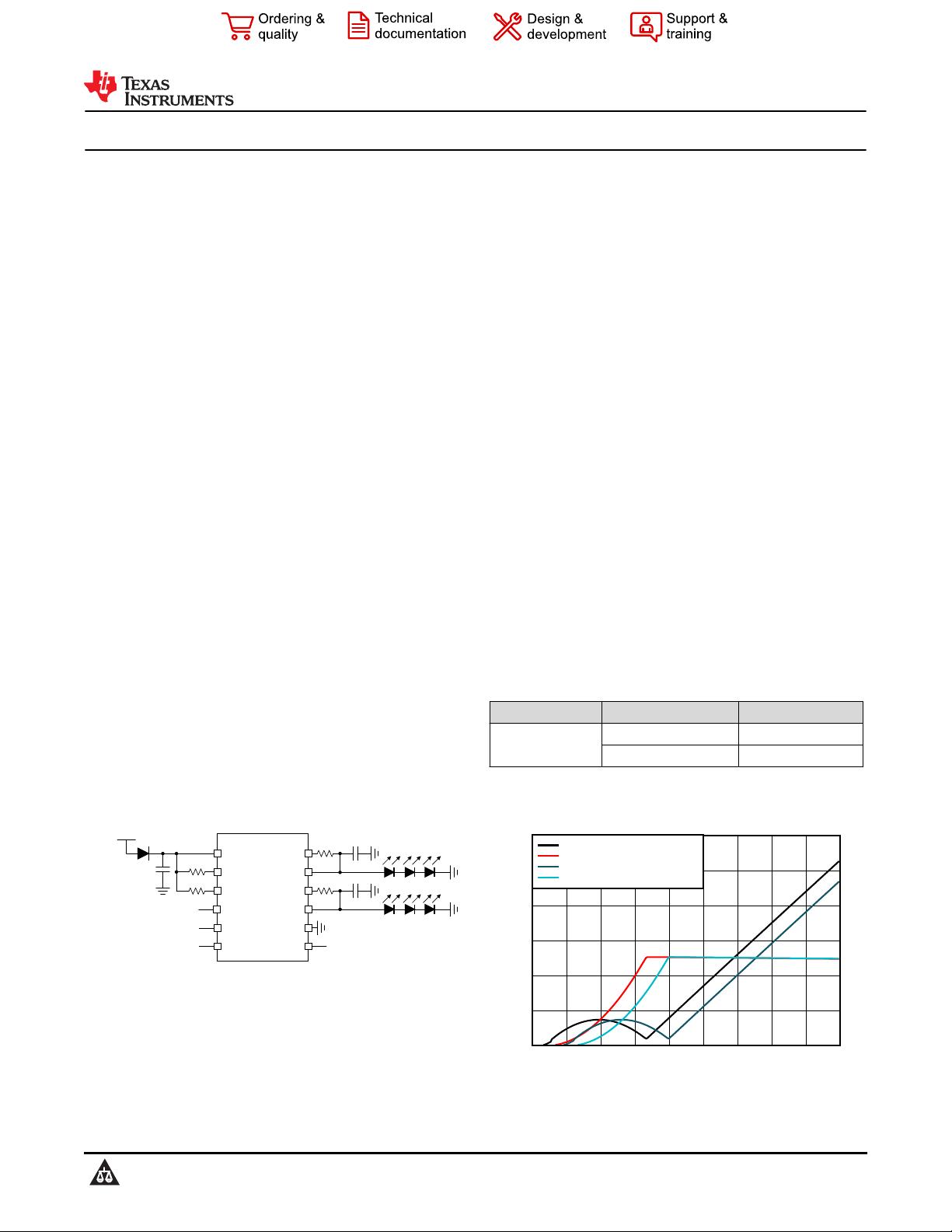
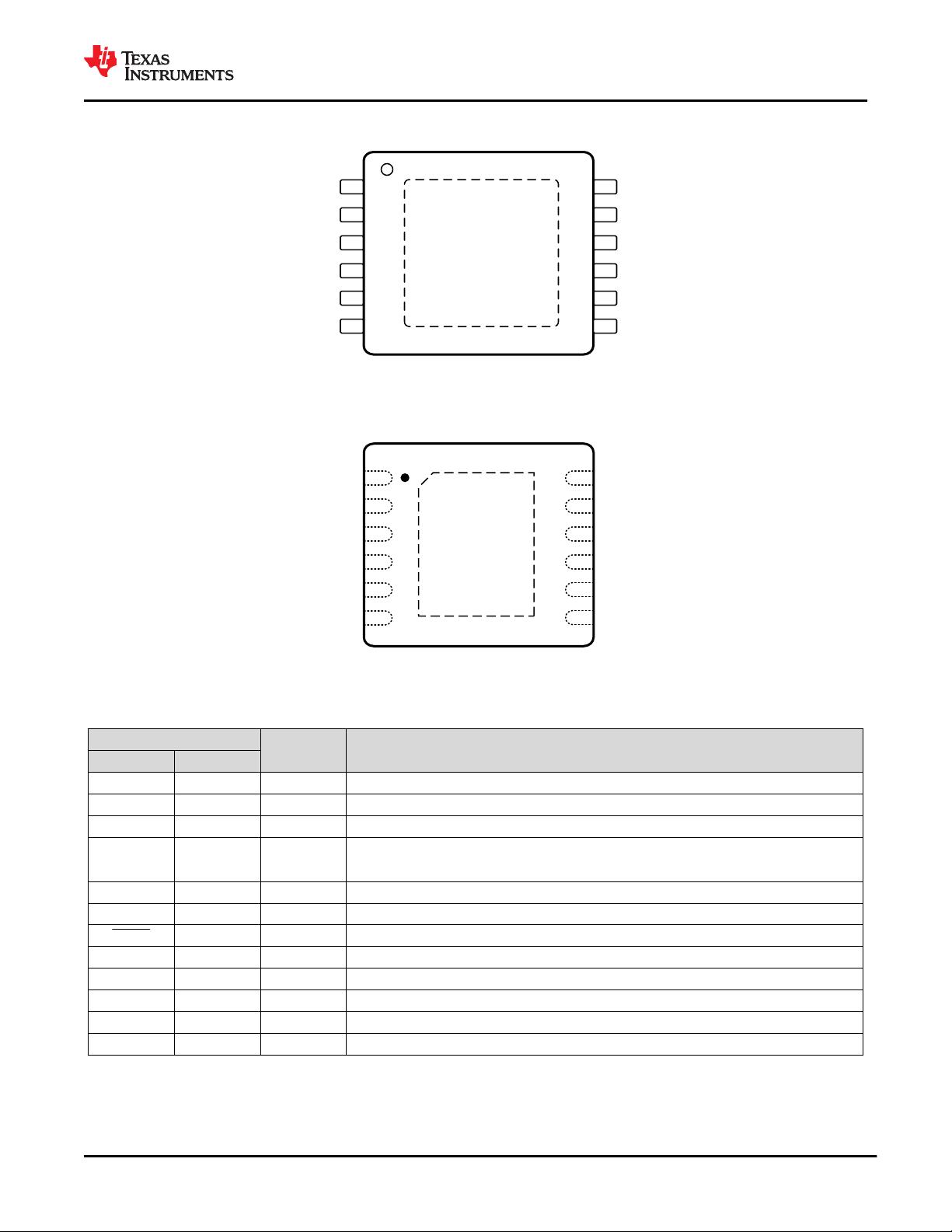
IN1
IN2
PWM1
PWM2
RES1
OUT1
RES2
OUT2
SUPPLY
DIAGEN
GND
TPS92622-Q1
4.5 V to 40 V
R
(SNS1)
R
(SNS2)
C
(SUPPLY)
R
(RES1)
R
(RES2)
C
(OUT1)
C
(OUT2)
FAULT
Typical Application Diagram
Supply Voltage (V)
Power (W) 150mA/Channel
3 6 9 12 15 18 21 24 27 30
0
0.5
1
1.5
2
2.5
3
P
(DEVICE)
R
(RESx)
= 55 2LEDs
P
(RESx)
R
(RESx)
= 55 2LEDs
P
(DEVICE)
R
(RESx)
= 55 3LEDs
P
(RESx)
R
(RESx)
= 55 3LEDs
Power Dissipation on Device
TPS92622-Q1
SLVSGW4 – NOVEMBER 2022
An IMPORTANT NOTICE at the end of this data sheet addresses availability, warranty, changes, use in safety-critical applications,
intellectual property matters and other important disclaimers. PRODUCTION DATA.


 我的内容管理
展开
 我的资源
快来上传第一个资源
 我的收益 登录查看自己的收益
 我的积分
登录查看自己的积分
 我的C币
登录后查看C币余额
 我的收藏
我的收藏  我的下载
我的下载  下载帮助
下载帮助 
 前往需求广场,查看用户热搜
 信息提交成功

