MAX1838EEE maxim 美信芯片 电子元器件中文版规格手册.pdf
需积分: 5 184 浏览量
2023-06-07
10:02:15
上传
评论
收藏 316KB PDF 举报


General Description
The MAX1838 is a dual, current-limited USB switch with
auxiliary input supply. Each switch meets all IEC speci-
fications for USB ports and is guaranteed to supply
500mA from either of two input supplies. A control pin
selects the power source from either the main or auxil-
iary supply.
The MAX1838 has multiple protection features, includ-
ing independent thermal-shutdown on each channel to
limit junction temperature in case of a prolonged short
or overload condition. The device has accurate internal
current-limit and reverse-current protection to safe-
guard the input supply against overload. When pow-
ered from the auxiliary supply, the current limit on each
channel is set independently with an external resistor.
An autoreset feature latches the switch off if the output
is shorted, thereby saving system power. When the
short is removed, the switch automatically turns back
on. Independent fault signals (FAULTA and FAULTB)
notify the microprocessor (µP) that the internal current
limit has been reached. A 20ms fault-blanking feature
prevents the MAX1838 from issuing false alarms to the
host during power-up or when hot-swapping into a
capacitive load.
The MAX1838 is available in a space-saving 16-pin
QSOP. For other USB current-limited switches, refer to
the MAX1693, MAX1694, MAX1812, and MAX1823.
Applications
Desktops
Notebook Computers
USB Ports
Docking Stations
Features
o Dual USB Switch with Auxiliary Input
o Autoreset from Fault Condition
o Guaranteed 500mA Load per Channel
o Programmable Current Limits on Auxiliary Inputs
o Reverse Current Protection
o Thermal Overload Protection
o Built-In 20ms Fault-Blanking
o 4V to 5.5V Range
o Independent FAULT Indicator Outputs
MAX1838
Dual USB Switch with Fault Blanking
and Autoreset
________________________________________________________________
Maxim Integrated Products
1
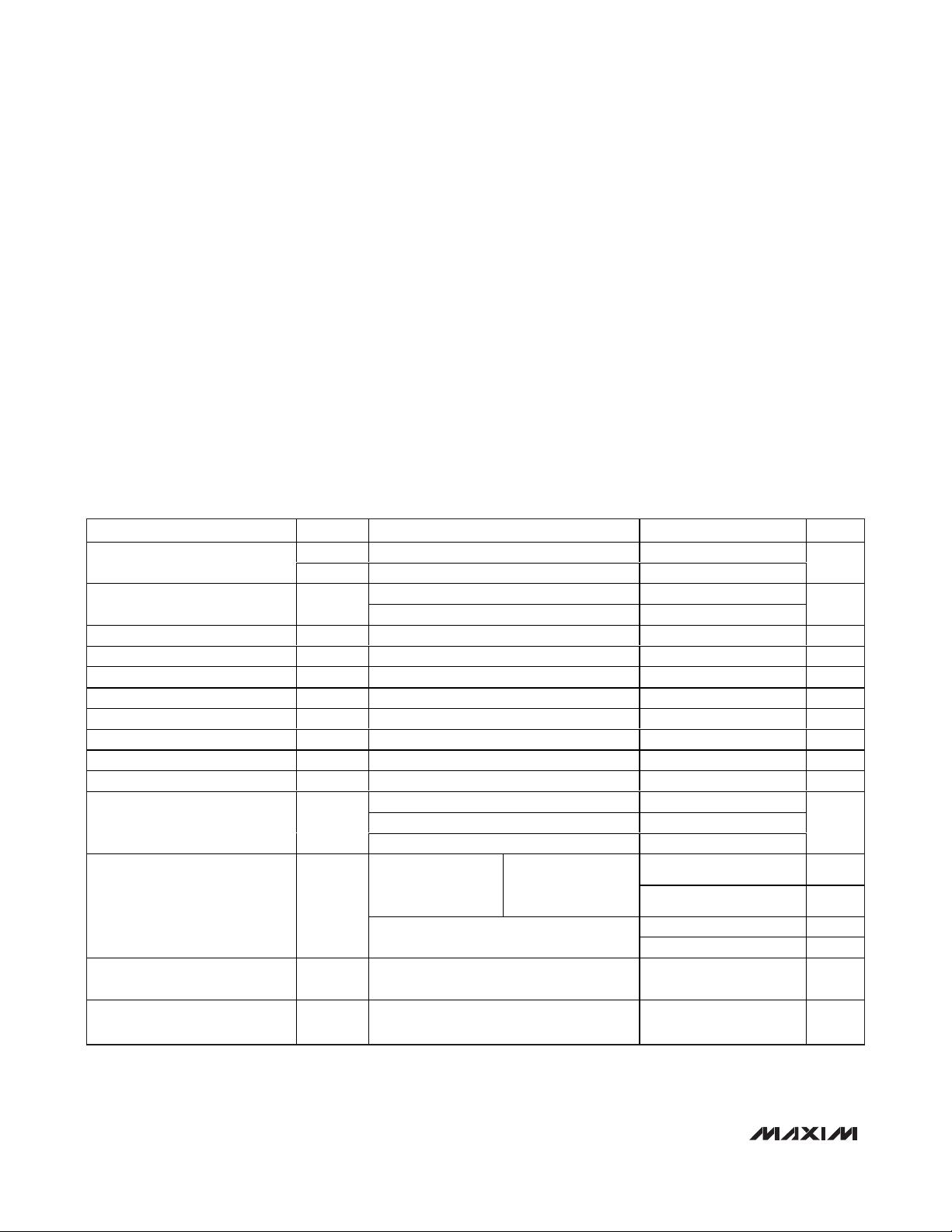
16
15
14
13
12
11
10
9
1
2
3
4
5
6
7
8
GND FAULTA
ADJA
OUTA2
OUTA1
OUTB2
OUTB1
ADJB
FAULTB
TOP VIEW
MAX1838
QSOP
SEL
AUXA
AUXB
INA
INB
ON
GND
Pin Configuration
Ordering Information
19-2033; Rev 1; 2/10
PART TEMP RANGE PIN-PACKAGE
MAX1838EEE -40°C to +85°C 16 QSOP
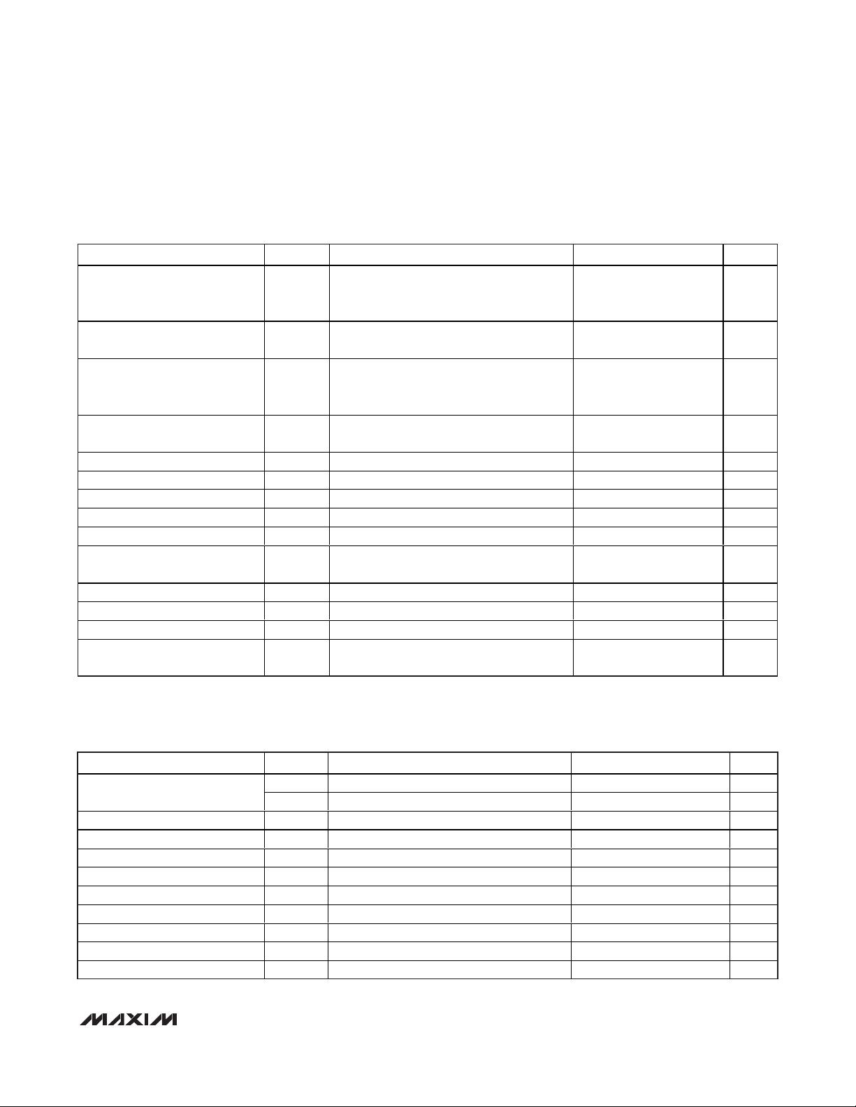
FAULTB
FAULTA
OUTB
OUTA
ADJB
ADJA
AUXA
AUXB
INA
INB
SEL
ON
GND
AUX
IN
OUTB
OUTA
10µF
MAX1838
Typical Operating Circuit
For pricing, delivery, and ordering information, please contact Maxim Direct at 1-888-629-4642,
or visit Maxim’s website at www.maxim-ic.com.
剩余13页未读,继续阅读
资源评论


