没有合适的资源?快使用搜索试试~ 我知道了~
MAX1748EUE maxim 美信芯片 电子元器件中文版规格手册.pdf
需积分: 5 1 下载量 158 浏览量
2023-06-06
10:21:20
上传
评论
收藏 224KB PDF 举报
温馨提示
试读
17页
MAX1748EUE maxim 美信芯片 电子元器件中文版规格手册
资源推荐
资源详情
资源评论
General Description
The MAX1748/MAX8726 triple-output DC-DC converters
in a low-profile TSSOP package provide the regulated
voltages required by active-matrix, thin-film transistor
(TFT) liquid-crystal displays (LCDs). One high-power
DC-DC converter and two low-power charge pumps
convert the +3.3V to +5V input supply voltage into three
independent output voltages.
The primary 1MHz DC-DC converter generates a boost-
ed output voltage (V
MAIN
) up to 13V using ultra-small
inductors and ceramic capacitors. The low-power
BiCMOS control circuitry and the low on-resistance
(0.35Ω) of the integrated power MOSFET allows effi-
ciency up to 93%.
The dual charge pumps independently regulate one
positive output (V
POS
) and one negative output (V
NEG
).
These low-power outputs use external diode and
capacitor stages (as many stages as required) to regu-
late output voltages up to +40V and down to -40V. A
proprietary regulation algorithm minimizes output rip-
ple, as well as capacitor sizes for both charge pumps.
For both the MAX1748 and MAX8726, the supply
sequence is V
MAIN
first, V
NEG
next, and finally V
POS
.
The MAX1748 soft-starts each supply as soon as the
previous supply finishes. The MAX8726 adds a delay
between the startups of V
MAIN
and V
NEG
and also
between V
NEG
and V
POS
.
The MAX1748/MAX8726 are available in the ultra-thin
TSSOP package (1.1mm max height).
Applications
TFT Active-Matrix LCD Displays
Passive-Matrix LCD Displays
PDAs
Digital Still Cameras
Camcorders
Features
♦ Three Integrated DC-DC Converters
♦ 1MHz Current-Mode PWM Boost Regulator
Up to +13V Main High-Power Output
±1% Accuracy
High Efficiency (93%)
♦ Dual Charge-Pump Outputs
Up to +40V Positive Charge-Pump Output
Down to -40V Negative Charge-Pump Output
♦ Internal Supply Sequencing
♦ Internal Power MOSFETs
♦ +2.7V to +5.5V Input Supply
♦ 0.1µA Shutdown Current
♦ 0.6mA Quiescent Current
♦ Internal Soft-Start
♦ Power-Ready Output
♦ Ultra-Small External Components
♦ Thin TSSOP Package (1.1mm max)
MAX1748/MAX8726
Triple-Output TFT-LCD
DC-DC Converters
________________________________________________________________ Maxim Integrated Products 1
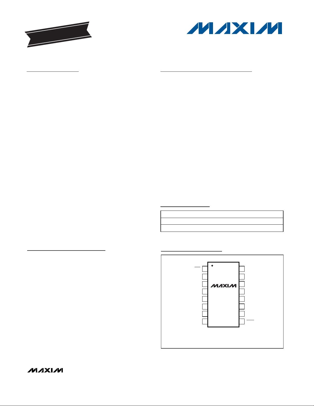
16
15
14
13
12
11
10
9
1
2
3
4
5
6
7
8
RDY TGND
LX
PGND
SUPP
DRVP
SUPN
DRVN
SHDN
TOP VIEW
MAX1748
MAX8726
TSSOP
FB
INTG
REF
IN
GND
FBP
FBN
A "+" SIGN WILL REPLACE THE FIRST PIN INDICATOR ON LEAD-FREE PACKAGES.
Pin Configuration
19-3430; Rev 0; 10/04
For free samples and the latest literature, visit www.maxim-ic.com or phone 1-800-998-8800.
For small orders, phone 1-800-835-8769.
EVALUATION KIT
AVAILABLE
Ordering Information
Typical Operating Circuit appears at end of data sheet.
PART TEMP RANGE PIN-PACKAGE
MAX1748EUE -40°C to +85°C 16 TSSOP
MAX8726EUE -40°C to +85°C 16 TSSOP
MAX1748/MAX8726
Triple-Output TFT-LCD
DC-DC Converters
2 _______________________________________________________________________________________
ABSOLUTE MAXIMUM RATINGS
ELECTRICAL CHARACTERISTICS
(V
IN
= +3.0V, SHDN = IN, V
SUPP
= V
SUPN
= 10V, TGND = PGND = GND, C
REF
= 0.22µF, C
INTG
= 470pF, T
A
= 0°C to +85°C, unless
otherwise noted. Typical values are at T
A
= +25°C.)
Stresses beyond those listed under “Absolute Maximum Ratings” may cause permanent damage to the device. These are stress ratings only, and functional
operation of the device at these or any other conditions beyond those indicated in the operational sections of the specifications is not implied. Exposure to
absolute maximum rating conditions for extended periods may affect device reliability.
IN, SHDN, TGND to GND .........................................-0.3V to +6V
DRVN to GND .........................................-0.3V to (V
SUPN
+ 0.3V)
DRVP to GND..........................................-0.3V to (V
SUPP
+ 0.3V)
PGND to GND.....................................................................±0.3V
RDY to GND ...........................................................-0.3V to +14V
LX, SUPP, SUPN to PGND .....................................-0.3V to +14V
INTG, REF, FB, FBN, FBP to GND...............-0.3V to (V
IN
+ 0.3V)
Continuous Power Dissipation (T
A
= +70°C)
16-Pin TSSOP (derate 9.4mW/°C above +70°C) ..........755mW
Operating Temperature Range
MAX1748EUE/MAX8726EUE..........................-40°C to +85°C
Junction Temperature......................................................+150°C
Storage Temperature Range .............................-65°C to +150°C
Lead Temperature (soldering, 10s) .................................+300°C
PARAMETER
SYMBOL
CONDITIONS
MIN
TYP
MAX
UNITS
Input Supply Range V
IN
2.7 5.5 V
Input Undervoltage Threshold
V
UVLO
V
IN
rising, 40mV hysteresis (typ) 2.2 2.4 2.6 V
IN Quiescent Supply Current I
IN
V
FB
= V
FBP
= 1.5V, V
FBN
= -0.2V 0.6 1 mA
SUPP Quiescent Current I
SUPP
V
FBP
= 1.5V 0.4 0.8 mA
SUPN Quiescent Current I
SUPN
V
FBN
= -0.1V 0.4 0.8 mA
IN Shutdown Current V
SHDN
= 0, V
IN
= 5V 0.1 10 µA
SUPP Shutdown Current V
SHDN
= 0, V
SUPP
= 13V 0.1 10 µA
SUPN Shutdown Current V
SHDN
= 0, V
SUPN
= 13V 0.1 10 µA
MAIN BOOST CONVERTER
Output Voltage Range
V
MAIN
V
IN
13 V
FB Regulation Voltage V
FB
T
A
= 0°C to +85°C
1.235 1.248 1.261
V
FB Input Bias Current I
FB
V
FB
= 1.25V, INTG = GND -50
+50
nA
Operating Frequency f
OSC
0.85
1
1.15
MHz
Oscillator Maximum Duty Cycle
78 85 90 %
Load Regulation I
MAIN
= 0 to 200mA, V
MAIN
= 10V 0.2 %
Line Regulation 0.1
% / V
Integrator Gm
320
µmho
LX Switch On-Resistance
R
LX
(
ON
)
I
LX
= 100mA
0.35
0.7 Ω
LX Leakage Current I
LX
V
LX
= 13V
0.01
20 µA
Phase I = soft-start (1.0ms)
0.275 0.380 0.500
Phase II = soft-start (1.0ms)
0.75
Phase III = soft-start (1.0ms)
1.12
LX Current Limit
I
LX
(
MAX
)
Phase IV = fully on (after 3.0ms) 1.1 1.5 2.0
A
Maximum RMS LX Current 1A
Soft-Start Period t
SS
Power-up to the end of phase III
3072 /
f
OSC
s
FB Fault Trip Level
1.07
1.1
1.14
V
POSITIVE CHARGE PUMP
V
SUPP
Input Supply Range
V
SUPP
2.7
13.0
V
MAX1748/MAX8726
Triple-Output TFT-LCD
DC-DC Converters
_______________________________________________________________________________________ 3
ELECTRICAL CHARACTERISTICS (continued)
(V
IN
= +3.0V, SHDN = IN, V
SUPP
= V
SUPN
= 10V, TGND = PGND = GND, C
REF
= 0.22µF, C
INTG
= 470pF, T
A
= 0°C to +85°C, unless
otherwise noted. Typical values are at T
A
= +25°C.)
PARAMETER
SYMBOL
CONDITIONS
MIN
TYP
MAX
UNITS
Operating Frequency
0.5 x
f
OSC
Hz
FBP Regulation Voltage V
FBP
1.20 1.25 1.30
V
FBP Input Bias Current I
FBP
V
FBP
= 1.5V -50
+50
nA
DRVP PCH On-Resistance
310 Ω
V
FBP
= 1.213V 1.5 4 Ω
DRVP NCH On-Resistance
V
FBP
= 1.275V 20 kΩ
FBP Power-Ready Trip Level Rising edge
1.091 1.125 1.159
V
FBP Fault Trip Level Falling edge
1.11
V
Maximum RMS DRVP Current 0.1 A
NEGATIVE CHARGE PUMP
V
SUPN
Input Supply Range
V
SUPN
2.7
13.0
V
Operating Frequency
0.5 x
f
OSC
Hz
FBN Regulation Voltage V
FBN
-50 0
+50
mV
FBN Input Bias Current I
FBN
V
FBN
= -0.05V -50
+50
nA
DRVN PCH On-Resistance
310 Ω
V
FBN
= 0.035V 1.5 4 Ω
DRVN NCH On-Resistance
V
FBN
= -0.025V 20 kΩ
FBN Power-Ready Trip Level Rising edge 80
110
165 mV
FBN Fault Trip Level Falling edge
130
mV
Maximum RMS DRVN Current 0.1 A
REFERENCE
Reference Voltage V
REF
-2µA < I
REF
< +50µA
1.231 1.25 1.269
V
Reference Undervoltage
Threshold
V
REF
rising 0.9
1.05
1.2 V
LOGIC SIGNALS
SHDN Input Low Voltage 0.4V hysteresis (typ) 0.9 V
SHDN Input High Voltage 2.1 V
SHDN Input Current
I
SHDN
0.01
1µA
RDY Output Low Voltage I
SINK
= 2mA
0.25
0.5 V
RDY Output High Voltage V
RDY
= 13V
0.01
1µA
剩余16页未读,继续阅读
资源评论
芯脉芯城
- 粉丝: 3
- 资源: 4031
上传资源 快速赚钱
- 我的内容管理 展开
- 我的资源 快来上传第一个资源
- 我的收益 登录查看自己的收益
- 我的积分 登录查看自己的积分
- 我的C币 登录后查看C币余额
- 我的收藏
- 我的下载
- 下载帮助
最新资源
- 论文(最终)_20240430235101.pdf
- 基于python编写的Keras深度学习框架开发,利用卷积神经网络CNN,快速识别图片并进行分类
- 最全空间计量实证方法(空间杜宾模型和检验以及结果解释文档).txt
- 5uonly.apk
- 蓝桥杯Python组的历年真题
- 2023-04-06-项目笔记 - 第一百十九阶段 - 4.4.2.117全局变量的作用域-117 -2024.04.30
- 前端开发技术实验报告:内含4四实验&实验报告
- Highlight Plus v20.0.1
- 林周瑜-论文.docx
资源上传下载、课程学习等过程中有任何疑问或建议,欢迎提出宝贵意见哦~我们会及时处理!
点击此处反馈
安全验证
文档复制为VIP权益,开通VIP直接复制
信息提交成功