MAX1845EEI maxim 美信芯片 电子元器件中文版规格手册.pdf
需积分: 5 6 浏览量
2023-06-07
10:02:17
上传
评论
收藏 465KB PDF 举报

For pricing, delivery, and ordering information, please contact Maxim/Dallas Direct! at
1-888-629-4642, or visit Maxim’s website at www.maxim-ic.com.
General Description
The MAX1845 is a dual PWM controller configured for
step-down (buck) topologies that provides high efficien-
cy, excellent transient response, and high DC output
accuracy necessary for stepping down high-voltage bat-
teries to generate low-voltage chipset and RAM power
supplies in notebook computers. The CS_ inputs can be
used with low-side sense resistors to provide accurate
current limits or can be connected to LX_, using low-side
MOSFETs as current-sense elements.
The on-demand PWM controllers are free running, con-
stant on-time with input feed-forward. This configuration
provides ultra-fast transient response, wide input-output
differential range, low supply current, and tight load-reg-
ulation characteristics. The MAX1845 is simple and easy
to compensate.
Single-stage buck conversion allows the MAX1845 to
directly step down high-voltage batteries for the highest
possible efficiency. Alternatively, two-stage conversion
(stepping down the 5V system supply instead of the bat-
tery at a higher switching frequency) allows the minimum
possible physical size.
The MAX1845 is intended for generating chipset, DRAM,
CPU I/O, or other low-voltage supplies down to 1V. For a
single-output version, refer to the MAX1844 data sheet.
The MAX1845 is available in 28-pin QSOP and 36-pin
thin QFN packages.
Applications
Notebook Computers
CPU Core Supplies
Chipset/RAM Supply as Low as 1V
1.8V and 2.5V I/O Supplies
Features
♦ Ultra-High Efficiency
♦ Accurate Current-Limit Option
♦ Quick-PWM™ with 100ns Load-Step Response
♦ 1% V
OUT
Accuracy over Line and Load
♦ Dual Mode™ Fixed 1.8V/1.5V/Adj or 2.5V/Adj Outputs
♦ Adjustable 1V to 5.5V Output Range
♦ 2V to 28V Battery Input Range
♦ 200/300/420/540kHz Nominal Switching Frequency
♦ Adjustable Overvoltage Protection
♦ 1.7ms Digital Soft-Start
♦ Drives Large Synchronous-Rectifier FETs
♦ Power-Good Window Comparator
♦ 2V ±1% Reference Output
MAX1845
Dual, High-Efficiency, Step-Down
Controller with Accurate Current Limit
________________________________________________________________ Maxim Integrated Products 1
19-1955; Rev 2; 1/03
Pin Configurations appear at end of data sheet.
Quick-PWM and Dual Mode are trademarks of Maxim Integrated
Products.
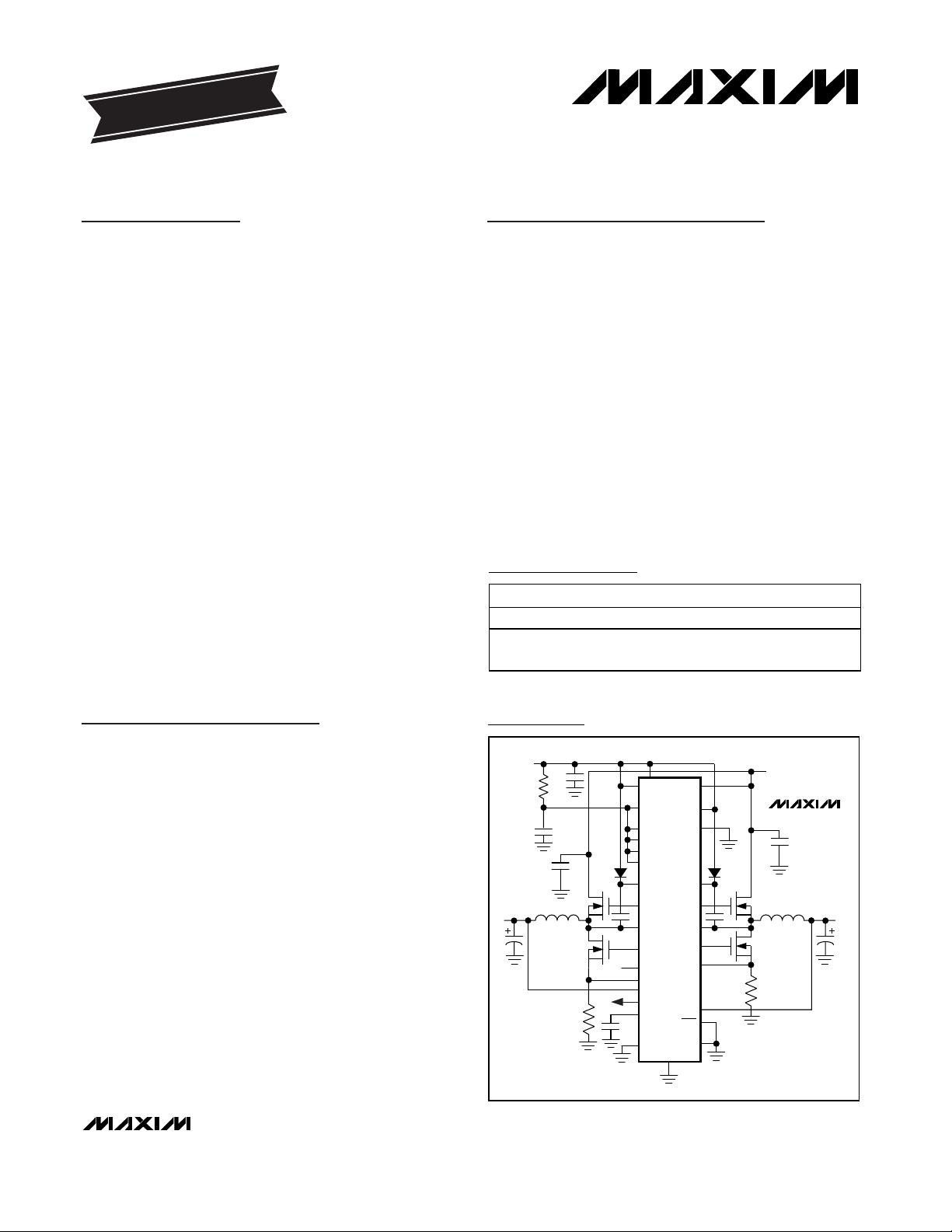
EVALUATION KIT
AVAILABLE
V
CC
OUTPUT1
1.8V
BATTERY
4.5V TO 28V
ILIM1
ON2
DL1
TON
OUT1
LX1
DH1
FB1
GND
V
DD
BST1
ILIM2
ON1
REF
DL2
CS2
OUT2
LX2
DH2
FB2
V+
BST2
SKIP
5V INPUT
PGOOD
OUTPUT2
2.5V
MAX1845EEI
UVP
OVP
CS1
Minimal Operating Circuit
Ordering Information
PART TEMP RANGE PIN-PACKAGE
MAX1845EEI
-40°C to +85°C 28 QSOP
MAX1845ETX
-40°C to +85°C
36 Thin QFN
6mm
✕ 6mm

剩余27页未读,继续阅读
资源评论


