MAX1820ZEUB maxim 美信芯片 电子元器件中文版规格手册.pdf
需积分: 5 190 浏览量
2023-06-07
10:02:14
上传
评论
收藏 616KB PDF 举报


General Description
The MAX1820/MAX1821 low-dropout, pulse-width-mod-
ulated (PWM) DC-DC buck regulators are optimized to
provide power to the power amplifier (PA) in WCDMA
cell phones; however, they may be applied in many
other applications where high efficiency is a priority. The
supply voltage range is from 2.6V to 5.5V, and the guar-
anteed output current is 600mA; 1MHz PWM switching
allows for small external components, while skip mode
reduces quiescent current to 180µA with light loads.
The MAX1820 is dynamically controlled to provide vary-
ing output voltages from 0.4V to 3.4V. The circuit is
designed such that the output voltage settles in <30µs
for a full-scale change in voltage and current. The
MAX1821 is set with external resistors to provide any
fixed output voltage in the 1.25V to 5.5V range.
The MAX1820/MAX1821 include a low on-resistance
internal MOSFET switch and synchronous rectifier to
maximize efficiency and minimize external component
count; 100% duty-cycle operation allows for low dropout
of only 150mV at 600mA load, including the external
inductor resistance. The devices are offered in 10-pin
µMAX
®
and tiny 3
✕
4 chip-scale (UCSP™) packages.
________________________Applications
WCDMA Cell Phone Power Amplifiers
PDA, Palmtop, and Notebook Computers
Microprocessor Core Supplies
Digital Cameras
PCMCIA and Network Cards
Hand-Held Instruments
Features
♦ Dynamically Adjustable Output from 0.4V to 3.4V
(MAX1820)
♦ Programmable Output from 1.25V to 5.5V
(MAX1821)
♦ SYNC to 13MHz External Clock (MAX1820X)
♦ SYNC to 19.8MHz External Clock (MAX1820Y)
♦ NO SYNC, Internal 1MHz Oscillator (MAX1820Z)
♦ Low Quiescent Current
180µA (typ) in Skip Mode
0.1µA (typ) in Shutdown Mode
♦ No External Schottky Diode Required
♦ 600mA Guaranteed Output Current
♦ 0% to 100% Duty-Cycle Operation
♦ 150mV Dropout at 600mA Load (Including R
DC
of External Inductor)
♦ µMAX or UCSP Packaging
MAX1820/MAX1821
WCDMA Cellular Phone 600mA
Buck Regulators
________________________________________________________________ Maxim Integrated Products 1
19-2011; Rev 3; 4/05
EVALUATION KIT
AVAILABLE
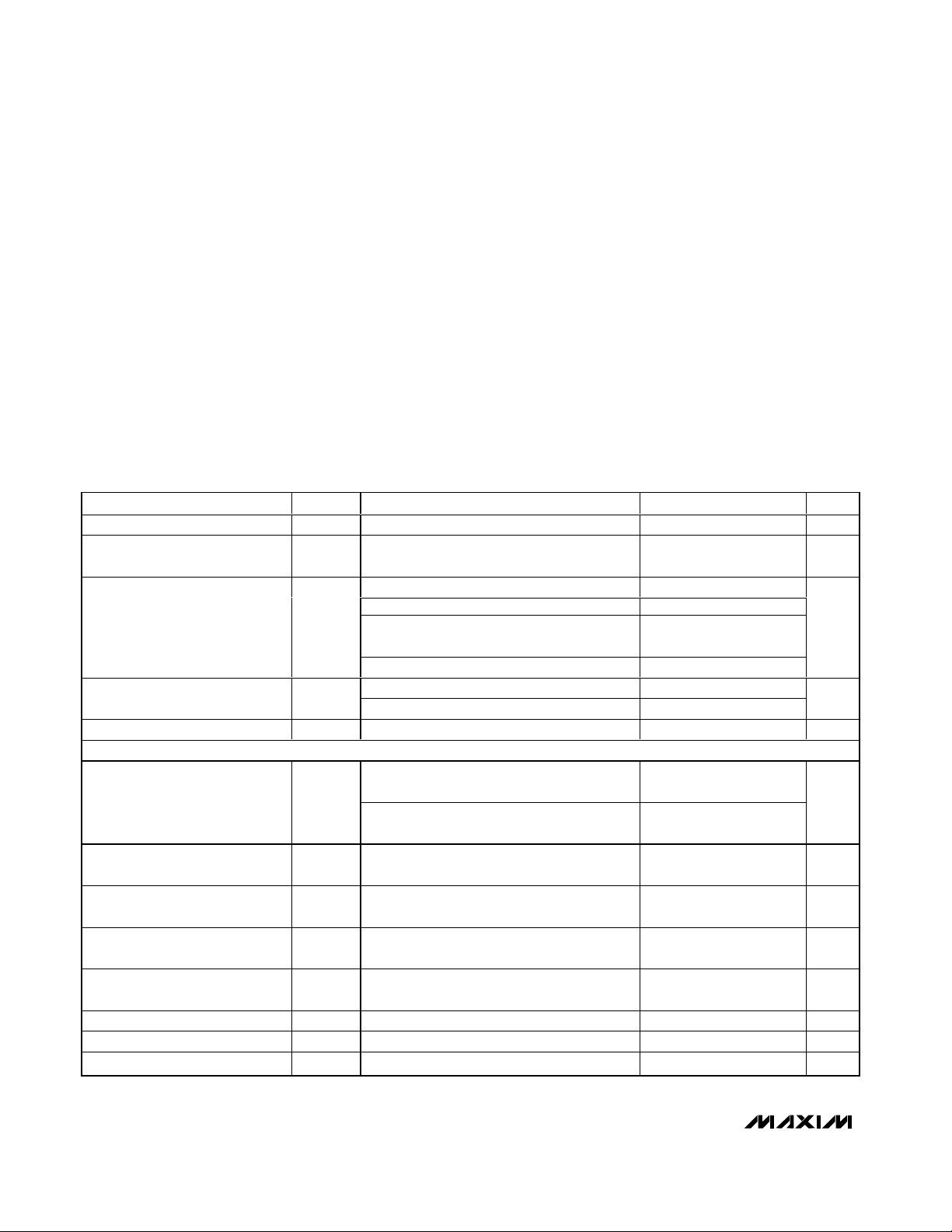
Ordering Information
PART
SYNC
FREQ (MHz)
OUTPUT VOLTAGE TEMP RANGE PIN-PACKAGE UCSP MARK
MAX1820ZEBC*
No Sync
Dynamic -40°C to +85°C 3
✕
4 UCSP AAB
MAX1820YEBC*
19.8
Dynamic -40°C to +85°C 3
✕
4 UCSP AAL
MAX1820XEBC*
13
Dynamic -40°C to +85°C 3
✕
4 UCSP AAM
MAX1820ZEUB
No Sync
Dynamic -40°C to +85°C 10 µMAX —
MAX1820YEUB
19.8
Dynamic -40°C to +85°C 10 µMAX —
MAX1820XEUB
13
Dynamic -40°C to +85°C 10 µMAX —
For pricing, delivery, and ordering information, please contact Maxim/Dallas Direct! at
1-888-629-4642, or visit Maxim’s website at www.maxim-ic.com.
Pin Configurations appear at end of data sheet.
Typical Operating Circuits continued at end of data sheet.
SYNC
GND
SHDN
BATT
PGND
COMP
V
OUT
CONTROL
DAC
REF
LX
OUT
13MHz
OR
19.8MHz
MAX1820
SKIP
4.7µH
4.7µF
INPUT
2.6V TO
5.5V
DYNAMIC
OUTPUT
0.4V TO 3.4V
Typical Operating Circuits
*UCSP reliability is integrally linked to the user’s assembly methods, circuit board material, and environment. See the UCSP Reliability
Notice in the UCSP Reliability section of this data sheet for more information.
UCSP is a trademark of Maxim Integrated Products, Inc.
µMAX is a registered trademark of Maxim Integrated Products, Inc.
Ordering Information continued at end of data sheet.
剩余18页未读,继续阅读
资源评论


