没有合适的资源?快使用搜索试试~ 我知道了~
MAX1874ETE maxim 美信芯片 电子元器件中文版规格手册.pdf
需积分: 5 0 下载量 6 浏览量
2023-06-07
10:02:18
上传
评论
收藏 899KB PDF 举报
温馨提示
试读
18页
MAX1874ETE maxim 美信芯片 电子元器件中文版规格手册
资源推荐
资源详情
资源评论
General Description
The MAX1874 charges a single-cell Li+ battery from
both USB and AC adapter sources. It also includes bat-
tery-to-input power switchover, so the system can be
powered directly from the power source rather than
from the battery.
In its simplest application, the MAX1874 needs no
external MOSFET or diodes, and accepts input volt-
ages up to 6.5V; however, DC input overvoltage protec-
tion up to 18V can be added with a single SOT PFET.
On-chip thermal limiting simplifies printed circuit board
(PCB) layout and allows optimum charging rate without
the thermal limits imposed by worst-case battery and
input voltage. When the MAX1874 thermal limit is
reached, the charger does not shut down but simply
reduces charging current.
Ambient or battery temperature can be monitored with
an external thermistor. When the temperature is out of
range, charging pauses.
Other features include a CHG output to indicate when
battery current tapers below a predetermined level. DC
power-OK (DCOK), USB power-OK (UOK), and power-
on (PON) outputs indicate when valid power is present.
These outputs drive logic or power-selection MOSFETs
to disconnect the charging sources from the load and
to protect the MAX1874 from overvoltage.
The MAX1874 contains no logic for communication with
the USB host. It must receive instructions from a local
microcontroller. The MAX1874 is available in a 16-pin
5mm ✕ 5mm thin QFN package and operates over the
-40°C to +85°C temperature range.
Applications
PDAs Cell Phones
Wireless Appliances Digital Cameras
Features
♦ Charge from USB or AC Adapter
♦ Automatic Switchover to AC Adapter
♦ Thermal Limiting Simplifies Board Design
♦ Small, High-Power 16-Pin Thin QFN Package
♦ Input Protection Up to 18V
♦ Soft-Start
♦ Automatic Battery-to-Input Load Switch
MAX1874
Dual-Input, USB/AC Adapter, 1-Cell
Li+ Charger with OVP and Thermal Regulation
________________________________________________________________ Maxim Integrated Products 1
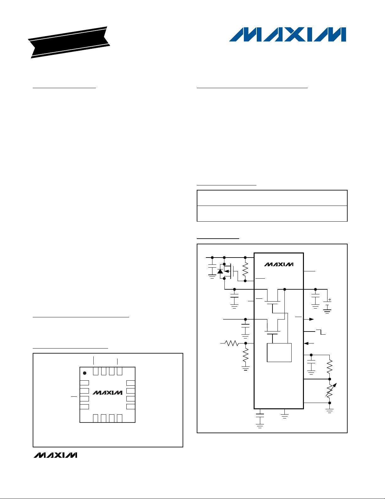
Ordering Information
19-2912; Rev 1; 2/07
For pricing, delivery, and ordering information, please contact Maxim/Dallas Direct! at
1-888-629-4642, or visit Maxim’s website at www.maxim-ic.com.
EVALUATION KIT
AVAILABLE
PART TEMP RANGE
PIN-
PACKAGE
PKG
CODE
MAX1874ETE
-40°C to +85°C
16 Thin QFN
5mm x 5mm
T1655-2
16 15 14 13
DCOK
BATT
PON
UOK
9
10
11
12
REF
PGND
BYP
USB
4
3
2
1
USEL
CHG
DC
DCLV
5678
EN
GND
DCI
THRM
MAX1874
THIN QFN
5mm x 5mm
TOP VIEW
Pin Configuration
Functional Diagram appears at the end of the data sheet.
MAX1874
USB INPUT
DC INPUT
TO REF
DCLV
GND
BATT
NTC
THERMISTOR
PON
REF
THRM
DC
USB
Li+
CELL
USEL
500mA
100mA
ENDCI
PGND
BYP
REGULATOR
UOK
CHG
DCOK
Typical Operating Circuit
MAX1874
Dual-Input, USB/AC Adapter, 1-Cell
Li+ Charger with OVP and Thermal Regulation
2 _______________________________________________________________________________________
ABSOLUTE MAXIMUM RATINGS
ELECTRICAL CHARACTERISTICS
(V
USB
= V
DC
= V
DCLV
= V
EN
= V
USEL
= 5V, V
BATT
= 4.2V, V
THRM
= V
REF
/ 2, Circuit of Figure 2, T
A
= 0°C to +85°C, unless otherwise
noted. Typical values are at T
A
= +25°C.)
Stresses beyond those listed under “Absolute Maximum Ratings” may cause permanent damage to the device. These are stress ratings only, and functional
operation of the device at these or any other conditions beyond those indicated in the operational sections of the specifications is not implied. Exposure to
absolute maximum rating conditions for extended periods may affect device reliability.
DC, DCOK to GND .................................................-0.3V to +20V
DCLV, BYP, USB, UOK, DCI, REF, USEL, THRM,
EN, BATT, CHG, PON to GND .............................-0.3V to +7V
PGND to GND .......................................................-0.3V to +0.3V
Continuous Current (DCLV) ..................................................1.1A
Continuous Current (USB) ....................................................0.6A
Continuous Power Dissipation (T
A
= +70°C)
16-Pin 5mm
✕ 5mm Thin QFN
(derate 21.3mW/°C above +70°C)...................................1.7W
Operating Temperature Range ...........................-40°C to +85°C
Storage Temperature Range .............................-65°C to +150°C
Maximum Junction Temperature .....................................+150°C
Lead Temperature (soldering, 10s) .................................+300°C
PARAMETER CONDITIONS
MIN TYP MAX
UNITS
INPUT VOLTAGE RANGES AND INPUT CURRENT
Maximum DC Input Voltage with
Overvoltage Protection
Q2 input MOSFET must be in place; charging
occurs only below 6.2V, Figures 3, 4, and 5
18 V
Maximum DC Input Voltage Without
Overvoltage Protection
DC = DCLV, Q2 input MOSFET not on circuit,
Figure 2
6.5 V
Maximum Input Voltage for Charging 6.0 6.2 6.5 V
V
EN
= 0V 2 4
DC Supply Current
V
EN
= 5V 4 6
mA
DCLV Operating Voltage Range
4.35 6.00
V
DCLV Shutdown Supply Current V
EN
= 0V
300
500 µA
USB Input Voltage Range
4.35 6.50
V
V
EN
= 0V
500
750 µA
V
EN
= 5V, V
DC
= 0V 2 3 mA
USB Supply Current
V
EN
= 5V, V
DC
= 5V
160
300 µA
DCI Input Current 1 100 nA
BYP Output Resistance (Note 1) 5 Ω
THRM Input Bias Current 1 100 nA
BATTERY VOLTAGE
BATT Regulation Voltage
4.1685 4.20 4.2315
V
BATT Prequal Voltage Threshold BATT rising 2.8 3 3.2 V
Prequal Threshold Hysteresis 70 mV
I
USB
= 100mA
100
USB Charging Headroom
I
USB
= 500mA
200
mV
DC Charging Headroom I
DCIN
= 800mA
250
mV
REF Voltage (Buffered Output)
I
REF
= 0 to 500µA, 4V < V
DC
or V
USB
< 6.5V;
does not affect BATT regulation accuracy
2.94
3
3.06
V
MAX1874
Dual-Input, USB/AC Adapter, 1-Cell
Li+ Charger with OVP and Thermal Regulation
_______________________________________________________________________________________ 3
ELECTRICAL CHARACTERISTICS (continued)
(V
USB
= V
DC
= V
DCLV
= V
EN
= V
USEL
= 5V, V
BATT
= 4.2V, V
THRM
= V
REF
/ 2, Circuit of Figure 2, T
A
= 0°C to +85°C, unless otherwise
noted. Typical values are at T
A
= +25°C.)
PARAMETER CONDITIONS
MIN TYP MAX UNITS
BATTERY CHARGING AND PRECHARGE CURRENT
DCI Voltage Range
0.1 x V
REF
V
REF
V
V
DCI
= V
REF
950 1000 1050
DCI Voltage to BATT Current
V
DCI
= V
REF
/ 2
490 520
550
mA
USEL = high
455
495
USB Charging Current
USEL = low 82 95
mA
Soft-Start Current-Ramp Time Measured from 10% to 90% 7 ms
Prequal Charging Current V
BATT
= 2.5V 35 55 70 mA
BATT Input Current No DC or USB power, V
BATT
= 4.2V 5 7.5 µA
BATT Shutdown Current EN = GND, USB- and/or DC-powered 1 2 µA
THERMISTOR MONITOR AND DIE-TEMPERATURE REGULATION
THRM COLD Trip Level (Note 2)
0.72 0.74 0.76 V
REF
THRM HOT Trip Level (Note 2)
0.28 0.29 0.30 V
REF
THRM Disable Threshold 50
100
150 mV
Internal Die Thermal Limit
+105
°C
LOGIC INPUT/OUTPUTS AND GATE DRIVERS
PON High Output Resistance
PON pulled up to active input (DCLV or USB),
V
DCLV
or V
USB
= 5V
25 Ω
PON Low Output Resistance PON resistance to GND, V
DCLV
= V
USB
= 0
120
kΩ
DCOK Low Output Resistance DCOK pulled low 25 Ω
DCOK Off-Leakage Current V
DCOK
= 12V, V
DC
= 0V 1 µA
UOK Output Resistance UOK resistance to GND, V
DC
= 0 25 Ω
UOK Off-Leakage Current V
UOK
= 6.5V 1 µA
DC input (% of charge current set at DCI) 8
12.5
19
U S B i np ut, U S E L = 5V ( % of U S B char g i ng cur r ent) 20 25 30
CHG Threshold to Indicate Battery Full,
Battery Current Falling (Note 3)
USB input with USEL = 0
Voltage
mode
%
CHG Logic-Low Output Sinking 10mA sink 0.4 V
CHG Leakage Current V
CHG
= 6.5V 1 µA
EN, USEL Logic-Input High Level 1.6 V
EN, USEL Logic-Input Low Level 0.4 V
EN, USEL Input Bias Current 1µA
MAX1874
Dual-Input, USB/AC Adapter, 1-Cell
Li+ Charger with OVP and Thermal Regulation
4 _______________________________________________________________________________________
ELECTRICAL CHARACTERISTICS (continued)
(V
USB
= V
DC
= V
DCLV
= V
EN
= V
USEL
= 5V, V
BATT
= 4.2V, V
THRM
= V
REF
/ 2, Circuit of Figure 2, T
A
= 0°C to +85°C, unless otherwise
noted. Typical values are at T
A
= +25°C.)
PARAMETER CONDITIONS
MIN
TYP
MAX
UNITS
TIMING
DC Rising to DCOK Falling USB = open, DC rising to 5V 20 ms
USB Rising to UOK Falling DC = open, USB rising to 5V 20 ms
DC Falling to DCOK Going
Open-Drain Propagation Delay
USB = open, 1kΩ pullup 2 µs
USB Falling to UOK Going
Open-Drain Propagation Delay
DC = open, 10kΩ pullup 2 µs
DC Rising to PON Rising (90%)
USB = open, DC step to 5V, BATT = 3.6V,
100kΩ pulldown
20 ms
USB Rising to PON Rising (90%)
DC = open, V
USB
step to 5V, V
BATT
= 3.6V,
100kΩ pulldown
20 ms
DC Falling to PON Going
Open-Drain Propagation Delay
USB = open, 100kΩ pulldown 2 µs
USB Falling to PON Going
Open-Drain Propagation Delay
DC = open, 100kΩ pulldown 2 µs
ELECTRICAL CHARACTERISTICS
(V
USB
= V
DC
= V
DCLV
= V
EN
= V
USEL
= 5V, V
BATT
= 4.2V, V
THRM
= V
REF
/ 2, Circuit of Figure 2, T
A
= -40°C to +85°C, unless otherwise
noted. Typical values are at T
A
= +25°C.) (Note 4)
PARAMETER CONDITIONS
MIN TYP MAX
UNITS
INPUT VOLTAGE RANGES AND INPUT CURRENT
Maximum DC Input Voltage with
Overvoltage Protection
Q2 input MOSFET must be in place; charging
occurs only below 6.2V, Figures 3, 4, and 5
18 V
Maximum DC Input Voltage Without
Overvoltage Protection
DC = DCLV, Q2 input MOSFET not on circuit,
Figure 3
6.5 V
Maximum Input Voltage for Charging 6.0 6.5 V
V
EN
= 0V 4
DC Supply Current
V
EN
= 5V 6
mA
DCLV Operating Voltage Range
4.35 6.00
V
DCLV Shutdown Supply Current V
EN
= 0V 500 µA
USB Input Voltage Range
4.35 6.50
V
V
EN
= 0V 750 µA
V
EN
= 5V, V
DC
= 0V 3 mA
USB Supply Current
V
EN
= 5V, V
DC
= 5V 300 µA
DCI Input Current 100 nA
THRM Input Bias Current 100 nA
剩余17页未读,继续阅读
资源评论
芯脉芯城
- 粉丝: 3
- 资源: 4031
上传资源 快速赚钱
- 我的内容管理 展开
- 我的资源 快来上传第一个资源
- 我的收益 登录查看自己的收益
- 我的积分 登录查看自己的积分
- 我的C币 登录后查看C币余额
- 我的收藏
- 我的下载
- 下载帮助
最新资源
- VR开发的概要介绍与分析
- 自动驾驶定位系列教程七:点云畸变补偿.pdf
- HM2302D-VB一款N-Channel沟道SOT23的MOSFET晶体管参数介绍与应用说明
- HM2302B-VB一款N-Channel沟道SOT23的MOSFET晶体管参数介绍与应用说明
- springboot学生考勤管理系统
- HM2302A-VB一款N-Channel沟道SOT23的MOSFET晶体管参数介绍与应用说明
- HM2301-VB一款P-Channel沟道SOT23的MOSFET晶体管参数介绍与应用说明
- 数据可视化的概要介绍与分析
- HM2301E-VB一款P-Channel沟道SOT23的MOSFET晶体管参数介绍与应用说明
- HM2301D-VB一款P-Channel沟道SOT23的MOSFET晶体管参数介绍与应用说明
资源上传下载、课程学习等过程中有任何疑问或建议,欢迎提出宝贵意见哦~我们会及时处理!
点击此处反馈
安全验证
文档复制为VIP权益,开通VIP直接复制
信息提交成功