没有合适的资源?快使用搜索试试~ 我知道了~
MAX1812EUB maxim 美信芯片 电子元器件中文版规格手册.pdf
需积分: 5 0 下载量 33 浏览量
2023-06-07
10:02:13
上传
评论
收藏 293KB PDF 举报
温馨提示
试读
11页
MAX1812EUB maxim 美信芯片 电子元器件中文版规格手册
资源推荐
资源详情
资源评论
For price, delivery, and to place orders, please contact Maxim Distribution at 1-888-629-4642,
or visit Maxim’s website at www.maxim-ic.com.
General Description
The MAX1812 is a dual current-limited switch specifi-
cally made for USB applications. Each channel is guar-
anteed to supply 500mA and meets USB specifications.
The MAX1812’s low quiescent supply current (45µA)
and shutdown current (3µA) conserve battery power in
portable applications.
The MAX1812 has multiple safety features to ensure
that the USB port is protected. Built-in thermal-overload
protection limits power dissipation and junction temper-
ature. The device also has accurate internal current-lim-
iting circuitry to protect the input supply against both
overload and short-circuit conditions. Independent fault
signals (FAULTA and FAULTB) notify the microproces-
sor when a thermal-overload, current limit, undervoltage
lockout, or short-circuit fault occurs. A 20ms fault-blank-
ing feature enables the circuit to ignore momentary
faults, such as those caused when hot-swapping a
capacitive load, thereby preventing false alarms to the
host system.
The MAX1812 is available in a space-saving 10-pin
µMAX package. For single versions of this device, refer
to the MAX1693, MAX1694, and MAX1607 data sheets.
________________________Applications
USB Ports
USB Hubs
Notebook Computers
Desktop Computers
PDAs and Palmtop Computers
Docking Stations
Features
♦ Dual USB Switch in Tiny 10-Pin µMAX Package
♦ Guaranteed 500mA Load per Channel
♦ Built-In 20ms Fault Blanking
♦ Compliant to USB Specifications
♦ +4.0V to +5.5V Input Voltage Range
♦ 45µA Quiescent Current
♦ 3µA Shutdown Current
♦ Independent Shutdown Control
♦ Independent FAULT Indicator Outputs
♦ Thermal-Overload Protection
♦ UL Listing Pending
MAX1812
Dual USB Switch with Fault Blanking
________________________________________________________________ Maxim Integrated Products 1
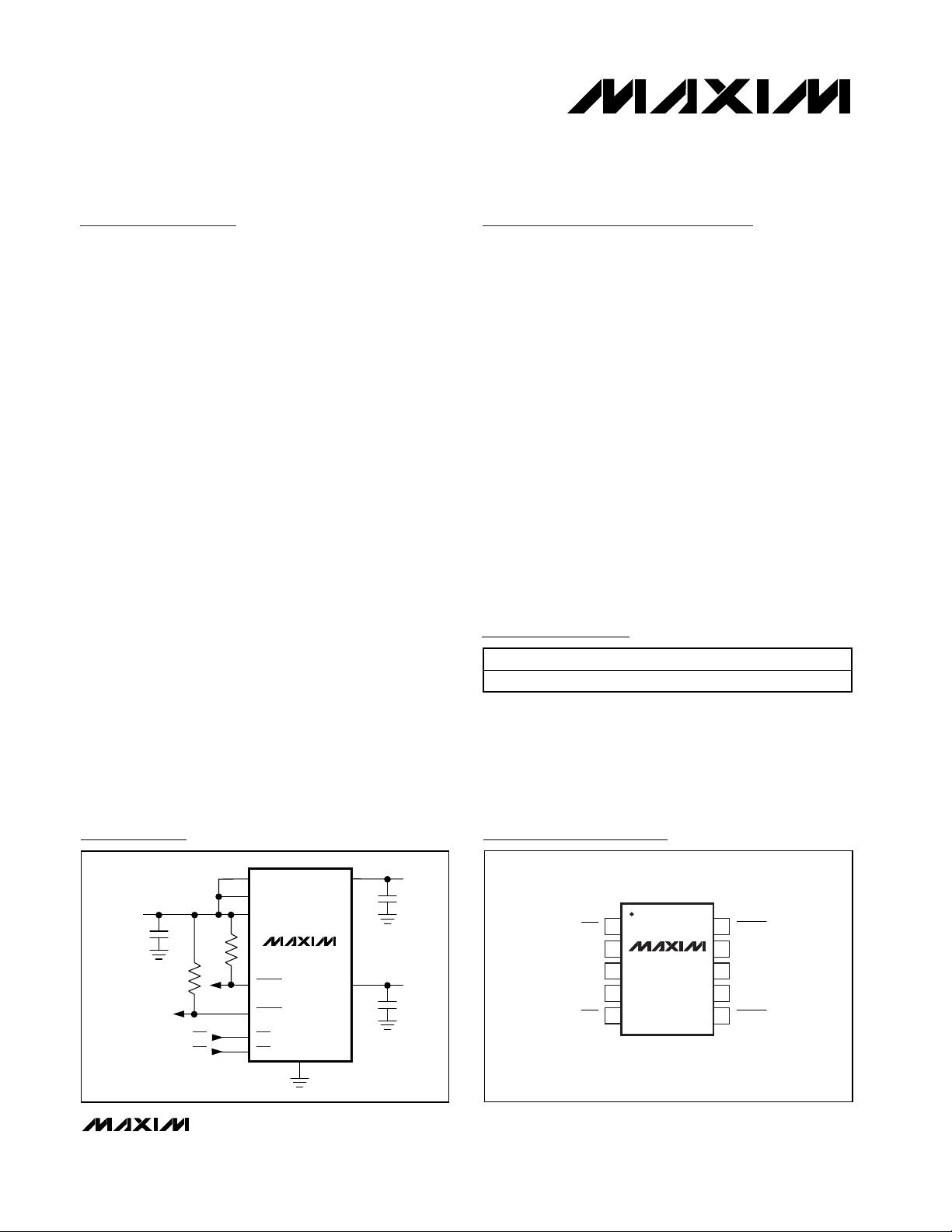
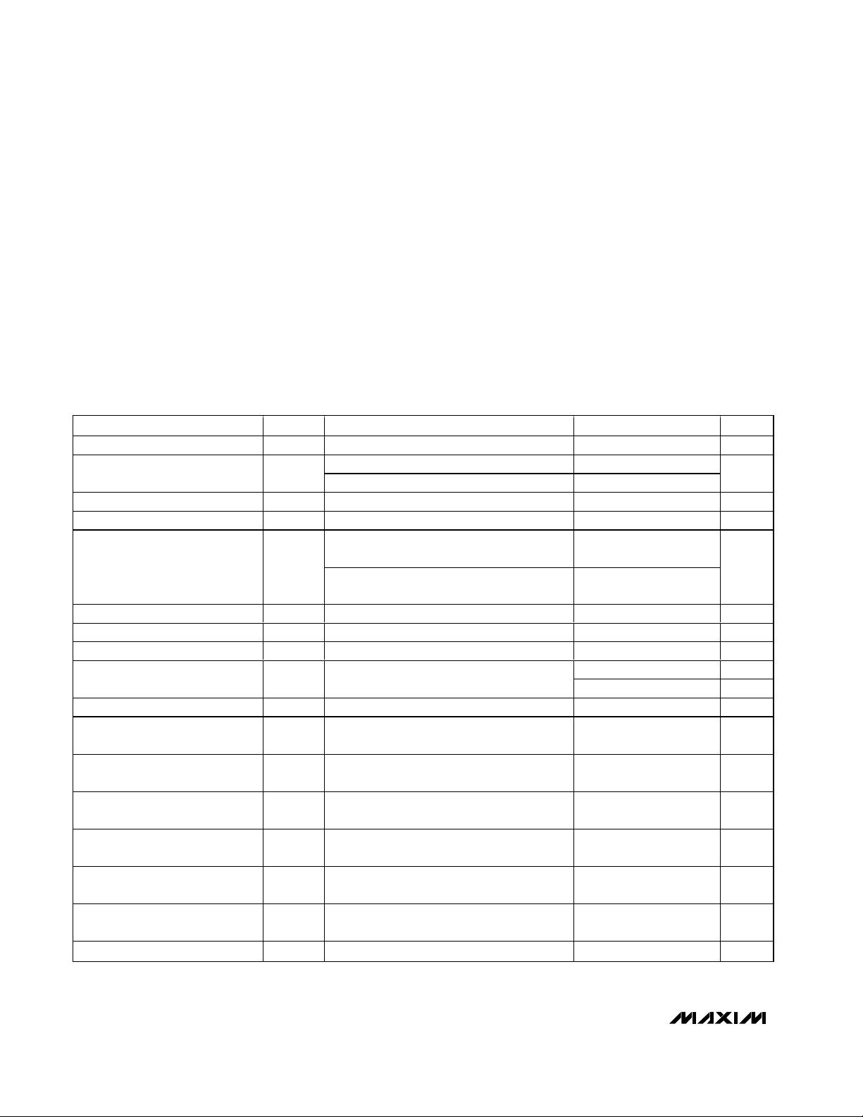
Pin Configuration
ONBONB
ONAONA
GND
MAX1812
FAULTB
FAULTA
IN
INA
INB
USB
PORT A
OUTA
USB
PORT B
OUTB
INPUT
4.0V TO 5.5V
Typical Operating Circuit
19-1865; Rev 0; 11/00
1
2
3
4
5
10
9
8
7
6
OUTA
GND
OUTBINB
IN
INA
MAX1812
µMAX
TOP VIEW
ONA
ONB FAULTB
FAULTA
Ordering Information
PART TEMP. RANGE PIN-PACKAGE
MAX1812EUB -40°C to +85°C 10 µMAX
MAX1812
Dual USB Switch with Fault Blanking
2 _______________________________________________________________________________________
ABSOLUTE MAXIMUM RATINGS
ELECTRICAL CHARACTERISTICS
(V
IN
= V
INA
= V
INB
= 5V, T
A
= -40°C to +85°C, unless otherwise noted. Typical values are at T
A
= +25°C) (Note 1)
Stresses beyond those listed under “Absolute Maximum Ratings” may cause permanent damage to the device. These are stress ratings only, and functional
operation of the device at these or any other conditions beyond those indicated in the operational sections of the specifications is not implied. Exposure to
absolute maximum rating conditions for extended periods may affect device reliability.
IN, INA, INB, ONA, ONB, OUTA, OUTB to GND......-0.3V to +6V
FAULTA, FAULTB to GND .........................-0.3V to (V
IN
_ + 0.3V)
INA, IN to OUTA; INB, IN to OUTB..........................-0.3V to +6V
OUTA, OUTB Maximum Continuous Switch Current
(per channel, internally limited) .........................................1.2A
FAULTA, FAULTB Current .................................................20mA
Continuous Power Dissipation (T
A
= +70°C)
10-Pin µMAX (derate 5.6mW/°C above +70°C) ............444mW
Operating Temperature Range ...........................-40°C to +85°C
Junction Temperature......................................................+150°C
Storage Temperature Range .............................-65°C to +150°C
Lead Temperature (soldering, 10s) .................................+300°C
PARAMETER SYMBOL CONDITIONS MIN TYP MAX UNITS
Supply Voltage Range 4.0 5.5 V
T
A
= +25°C, each switch 75 105
Switch On-Resistance R
ON
T
A
= -40°C to +85°C, each switch 135
mΩ
Standby Supply Current Both switches disabled 3 10 µA
Quiescent Supply Current Both switches enabled, I
OUTA
= I
OUTB
= 0 45 100 µA
Switches disabled, V
OUTA
= V
OUTB
= 0,
T
A
= +25°C
0.002 1
OUT_ Leakage Current
Switches disabled, V
OUTA
= V
OUTB
= 0,
T
A
= -40°C to 85°C
10
µA
U nd er vol tag e Lockout Thr eshol d UVLO Rising edge, 3% hysteresis 3.0 3.4 3.8 V
Continuous Load Current 500 mA
Continuous Current Limit ILIM V
IN
_ - V
OUT
_ = 0.5V 0.6 0.9 1.2 A
0.8 1.2 1.6 A( peak)
Short-Circuit Current Limit ISHORT V
OUT
_ = 0 (I
OUT
pulsing)
0.35 A
RMS
Short-Circuit Detect Threshold (Note 2) 1 V
Continuous Current-Limit
Blanking Timeout Period
From continuous current-limit condition to
FAULT_ assertion
10 20 35 ms
Short-Circuit Blanking Timeout
Period
From short-circuit current-limit condition to
FAULT_ assertion
7.5 18 35 ms
Turn-On Delay
R
OUT
= 10Ω, C
OUT
= 1µF does not include
rise time (from ON_ to 10% of V
OUT
)
0.5 1.2 4.0 ms
Output Rise Time
R
OUT
= 10Ω, C
OUT
= 1µF, from 10% to
90% of V
OUT
2.5 ms
Turn-Off Delay from ON
R
OUT
= 10Ω, C
OUT
= 1µF does not include
fall time (from ON_ to 90% of V
OUT
)
0.8 3 ms
Output Fall Time
C
OUT
= 1µF, R
OUT
= 10Ω, from 90% to 10%
of V
OUT
2.5 ms
Thermal Shutdown Threshold 15°C hysteresis 160 °C
MAX1812
Dual USB Switch with Fault Blanking
_______________________________________________________________________________________ 3
ELECTRICAL CHARACTERISTICS (continued)
(V
IN
= V
INA
= V
INB
= 5V, T
A
= -40°C to +85°C, unless otherwise noted. Typical values are at T
A
= +25°C.) (Note 1)
PARAMETER SYMBOL CONDITIONS MIN TYP MAX UNITS
Logic Input High Voltage V
IN_
= +4V to +5.5V 2 V
Logic Input Low Voltage V
IN_
= +4V to +5.5V 0.8 V
Logic Input Current V
ON_
= 0 or V
IN_
-1 1 µA
FAULT_ Output Low Voltage I
SINK
= 1mA, V
IN_
= 4V 0.4 V
FAULT_ Output High Leakage
Current
V
IN_
= V
FAULT_
= 5.5V 1 µA
Note 1: Specifications to -40°C are guaranteed by design, not production tested.
Note 2: The output voltage at which the device transitions from short-circuit current limit to continuous current limit.
Typical Operating Characteristics
(V
IN
= V
INA
= V
INB
= 5V, Circuit of Figure 2, T
A
= +25°C, unless otherwise noted.)
100
75
50
25
0
0312 456
QUIESCENT CURRENT
vs. INPUT VOLTAGE
MAX1812 toc01
INPUT VOLTAGE (V)
QUIESCENT CURRENT (µA)
V
ONA
= V
ONB
= 0V
40
45
50
55
-40 10-15 35 60 85
QUIESCENT CURRENT
vs. TEMPERATURE
MAX1812 toc02
TEMPERATURE (°C)
QUIESCENT CURRENT (µA)
V
IN
= 4.5V
V
IN
= 5V
V
IN
= 5.5V
0
1
2
3
4
5
-40 10-15 35 60 85
SHUTDOWN SUPPLY CURRENT
vs. TEMPERATURE
MAX1812 toc03
TEMPERATURE (°C)
SHUTDOWN SUPPLY CURRENT (µA)
V
ONA
= V
ONB
= V
IN
剩余10页未读,继续阅读
资源评论
芯脉芯城
- 粉丝: 3
- 资源: 4031
上传资源 快速赚钱
- 我的内容管理 展开
- 我的资源 快来上传第一个资源
- 我的收益 登录查看自己的收益
- 我的积分 登录查看自己的积分
- 我的C币 登录后查看C币余额
- 我的收藏
- 我的下载
- 下载帮助
最新资源
- 论文(最终)_20240430235101.pdf
- 基于python编写的Keras深度学习框架开发,利用卷积神经网络CNN,快速识别图片并进行分类
- 最全空间计量实证方法(空间杜宾模型和检验以及结果解释文档).txt
- 5uonly.apk
- 蓝桥杯Python组的历年真题
- 2023-04-06-项目笔记 - 第一百十九阶段 - 4.4.2.117全局变量的作用域-117 -2024.04.30
- 前端开发技术实验报告:内含4四实验&实验报告
- Highlight Plus v20.0.1
- 林周瑜-论文.docx
资源上传下载、课程学习等过程中有任何疑问或建议,欢迎提出宝贵意见哦~我们会及时处理!
点击此处反馈
安全验证
文档复制为VIP权益,开通VIP直接复制
信息提交成功