没有合适的资源?快使用搜索试试~ 我知道了~
MAX1791EUB maxim 美信芯片 电子元器件中文版规格手册.pdf
需积分: 5 0 下载量 16 浏览量
2023-06-07
10:02:11
上传
评论
收藏 656KB PDF 举报
温馨提示
试读
21页
MAX1791EUB maxim 美信芯片 电子元器件中文版规格手册
资源推荐
资源详情
资源评论
General Description
The MAX1762/MAX1791 PWM step-down controllers
provide high efficiency, excellent transient response,
and high DC output accuracy needed for stepping
down high-voltage batteries to generate low-voltage
CPU core, I/O, and chipset RAM supplies in notebook
computers and PDAs.
Maxim’s proprietary Quick-PWM™ pulse-width modula-
tor is a free-running constant on-time type with input
feed-forward. Its high operating frequency (300kHz)
allows small external components to be utilized in PC
board area-critical applications such as subnotebook
computers and smart phones. PWM operation occurs
at heavy loads, and automatic switchover to pulse-skip-
ping operation occurs at lighter loads. The external
high-side p-channel and low-side n-channel MOSFETs
require no bootstrap components. The MAX1762/
MAX1791 are simple, easy to compensate, and do not
have the noise sensitivity of conventional fixed-frequen-
cy current-mode PWMs.
These devices achieve high efficiency at a reduced
cost by eliminating the current-sense resistor found in
traditional current-mode PWMs. Efficiency is further
enhanced by their ability to drive synchronous-rectifier
MOSFETs. The MAX1762/MAX1791 come in a 10-pin
µMAX package and offer two fixed voltages (Dual
Mode™) for each device, 1.8V/2.5V/adj (MAX1762) and
3.3V/5.0V/adj (MAX1791).
________________________Applications
Notebooks Handy-Terminals
Subnotebooks PDAs
Digital Cameras Smart Phones
1.8V/2.5V Logic
and I/O Supplies
Features
♦ High Operating Frequency (300kHz)
♦ No Current-Sense Resistor
♦ Accurate Current Limit
♦ ±1% Total DC Error over Line and During
Continuous Conduction
♦ Dual Mode Fixed Output
1.8V/2.5V/adj (MAX1762)
3.3V/5.0V/adj (MAX1791)
♦ 0.5V to 5.5V Output Adjust Range
♦ 5V to 20V Input Range
♦ Automatic Light-Load Pulse Skipping Operation
♦ Free-Running On-Demand PWM
♦ Foldback Mode™ UVLO
♦ PFET/NFET Synchronous Buck
♦ 4.65V at 25mA Linear Regulator Output
♦ 5µA Shutdown Supply Current
♦ 230µA Quiescent Supply Current
♦ 10-Pin µMAX Package
MAX1762/MAX1791
High-Efficiency, 10-Pin µMAX, Step-Down
Controllers for Notebooks
________________________________________________________________ Maxim Integrated Products 1
19-1923; Rev 1; 10/05
EVALUATION KIT
AVAILABLE
Ordering Information
PART TEMP RANGE
PIN-PACKAGE
MAX1762EUB -40°C to +85°C 10 µMAX
MAX1791EUB -40°C to +85°C 10 µMAX
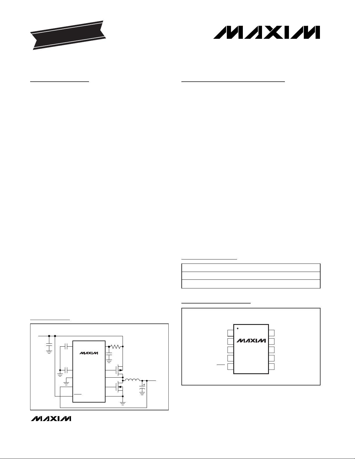
FB
GND
CS
DH
VP
DL
OUT
REF
SHDN
V
BATT
(5V TO 20V)
V
OUT
1.8V/3.3V
VL
MAX1762
MAX1791
Typical Operating Circuit
1
2
3
4
5
10
9
8
7
6
DH
CS
DLOUT
FB
REF
VL
MAX1762
MAX1791
µMAX
TOP VIEW
GNDSHDN
VP
Pin Configuration
For price, delivery, and to place orders, please contact Maxim Distribution at 1-888-629-4642,
or visit Maxim’s website at www.maxim-ic.com.
Quick-PWM, Dual Mode, and Foldback Mode are a trade-
marks of Maxim Integrated Products, Inc.
MAX1762/MAX1791
High-Efficiency, 10-Pin µMAX, Step-Down
Controllers for Notebooks
2 _______________________________________________________________________________________
ABSOLUTE MAXIMUM RATINGS
VP, SHDN to GND ..................................................-0.3V to +22V
VP to VL ..................................................................-0.3V to +22V
OUT, VL to GND .......................................................-0.3V to +6V
DL, FB, REF to GND ....................................-0.3V to (VL + 0.3V)
DH to GND....................................................-0.3V to (VP + 0.3V)
CS to GND ....................................................-2.0V to (VP + 0.3V)
REF Short Circuit to GND ...........................................Continuous
Continuous Power Dissipation (T
A
= +70°C)
10-Pin µMAX (derate 5.6mW/°C above +70°C) ...........444mW
Operating Temperature Range ...........................-40°C to +85°C
Junction Temperature......................................................+150°C
Storage Temperature Range .............................-65°C to +150°C
Lead Temperature (soldering, 10s) .................................+300°C
ELECTRICAL CHARACTERISTICS
(V
VP
= 15V, VL enabled, C
VL
= 1µF, C
REF
= 0.1µF,
T
A
= 0 to +85°C,
unless otherwise noted. Typical values are at T
A
= +25°C.)
(Note 1)
PARAMETER
SYMBOL
CONDITIONS
MIN TYP MAX
UNITS
VP Input Voltage Range V
VP
520V
VL Input Voltage Range V
VL
VL (overdriven)
4.75 5.25
V
OUT Output Voltage
(MAX1762, 1.8V Fixed)
V
OUT
V
VP
= 5V to 20V, V
VL
= 4.75V to 5.25V,
FB = GND, continuous conduction mode
1.773
1.8
1.827
V
OUT Output Voltage
(MAX1762, 2.5V Fixed)
V
OUT
V
VP
= 5V to 20V, V
VL
= 4.75V to 5.25V,
FB = VL, continuous conduction mode
2.463
2.5
2.538
V
OUT Output Voltage
(MAX1791, 3.3V Fixed)
V
OUT
V
VP
= 5V to 20V, V
VL
= 4.75V to 5.25V,
FB = GND, continuous conduction mode
3.250
3.3
3.350
V
OUT Output Voltage
(MAX1791, 5V Fixed)
V
OUT
V
VP
= 7V to 20V, V
VL
= 4.75V to 5.25V,
FB = VL, continuous conduction mode
4.925
5
5.075
V
OUT Output Voltage (Adj Mode)
V
VP
= 5V to 20V, V
VL
= 4.75V to 5.25V,
FB = OUT, continuous conduction mode
1.231 1.250 1.269
V
Output Voltage Adjust Range 0.5 5.5 V
OUT Input Resistance Adjustable-output mode
300 800 1700
kΩ
FB Input Bias Current V
FB
= 1.3V
-0.1
0.1 µA
Soft-Start Ramp Time Zero to full I
LIM
1700
µs
V
OUT
= 1.25V, V
VP
= 6V
666 740 814
On-Time (Note 2) t
ON
V
OUT
= 5V, V
VP
= 6V
2550 2830 3110
ns
Minimum Off-Time t
OFF
(Note 2)
300 400 500
ns
VL Quiescent Supply Current
FB = GND, V
VL
= 5V, OUT forced above the
regulation point
153 260
µA
V
VL
= float
227 410
VP Quiescent Supply Current
FB = GND, OUT forced
above the regulation point,
V
VP
= 20V
V
VL
= 5V 93
200
µA
VL Shutdown Supply Current V
VL
= 5V, SHDN = GND 2 15 µA
VP Shutdown Supply Current
S HD N = GN D , m easur ed at V P , V
V L
= 0 or 5V
412µA
VL Output Voltage I
LOAD
= 0 to 25mA, V
VP
= 5V to 20V 4.5
4.65 4.75
V
Stresses beyond those listed under “Absolute Maximum Ratings” may cause permanent damage to the device. These are stress ratings only, and functional
operation of the device at these or any other conditions beyond those indicated in the operational sections of the specifications is not implied. Exposure to
absolute maximum rating conditions for extended periods may affect device reliability.
MAX1762/MAX1791
High-Efficiency, 10-Pin µMAX, Step-Down
Controllers for Notebooks
_______________________________________________________________________________________ 3
ELECTRICAL CHARACTERISTICS (continued)
(V
VP
= 15V, VL enabled, C
VL
= 1µF, C
REF
= 0.1µF,
T
A
= 0 to +85°C,
unless otherwise noted. Typical values are at T
A
= +25°C.)
(Note 1)
PARAMETER
SYMBOL
CONDITIONS
MIN TYP MAX
UNITS
Reference Voltage V
VL
= 4.75V to 5.25V, no load
1.98
2
2.02
V
Reference Load Regulation I
REF
= 0 to 50µA
0.01
V
REF Sink Current REF in regulation 10 µA
REF Fault Lockout Voltage Falling edge 1.6 V
Output Undervoltage Threshold
(Foldback)
With respect to regulation point, no load 60 70 80 %
Output Undervoltage Lockout
Time (Foldback)
From SHDN signal going high V
OUT
< 0.6 x
regulation point
10 20 42 ms
Current-Limit Threshold V
ILIM
-90
-100 -110
mV
Thermal Shutdown Threshold Hysteresis = 10
o
C
160
o
C
VL Undervoltage Lockout
Threshold
Rising edge, hysteresis = 20mV, PWM
disabled below this level
4.1 4.4 V
DH Gate Driver On-Resistance V
VP
= 6V to 20V, measure at 50mA 5 8 Ω
DL Gate Driver On-Resistance
(Pullup)
DL, high state, measure at 50mA 5 8 Ω
DL Gate Driver On-Resistance
(Pulldown)
DL, low state, measure at 50mA 1 5 Ω
DH Gate Driver Source/Sink
Current
V
DH
= 3V, V
VP
= 6V 0.6 A
DL Gate Driver Sink Current V
DL
= 2.5V 0.9 A
DL Gate Driver Source Current V
DL
= 2.5V 0.5 A
SHDN Logic Input High
Threshold Voltage
V
IH
1.6 V
SHDN Logic Input Low
Threshold Voltage
V
IL
0.6 V
MAX1762 V
OUT
= 1.8V fixed
MAX1791 V
OUT
= 3.3V fixed
50
100 150
mV
MAX1762 V
OUT
= 2.5V fixed
Dual Mode Threshold Voltage
MAX1791 V
OUT
= 5V fixed
2.5
3.25
4V
SHDN Logic Input Current SHDN = 0 or 5V -2 +2 µA
MAX1762/MAX1791
High-Efficiency, 10-Pin µMAX, Step-Down
Controllers for Notebooks
4 _______________________________________________________________________________________
ELECTRICAL CHARACTERISTICS
(V
VP
= 15V, VL enabled, C
VL
= 1µF, C
REF
= 0.1µF,
T
A
= -40 to +85°C,
unless otherwise noted.) (Note 1)
PARAMETER
SYMBOL
CONDITIONS
MIN
TYP
MAX
UNITS
VP Input Voltage Range V
VP
520V
VL Input Voltage Range V
VL
VL (overdriven)
4.75 5.25
V
OUT Output Voltage
(MAX1762, 1.8V Fixed)
V
OUT
V
VP
= 5V to 20V, V
VL
= 4.75V to 5.25V,
FB = GND, continuous conduction mode
1.773 1.827
V
OUT Output Voltage
(MAX1762, 2.5V Fixed)
V
OUT
V
VP
= 5V to 20V, V
VL
= 4.75V to 5.25V,
FB = VL, continuous conduction mode
2.463 2.538
V
OUT Output Voltage
(MAX1791, 3.3V Fixed)
V
OUT
V
VP
= 5V to 20V, V
VL
= 4.75V to 5.25V,
FB = GND, continuous conduction mode
3.250 3.350
V
OUT Output Voltage
(MAX1791, 5V Fixed)
V
OUT
V
VP
= 7V to 20V, V
VL
= 4.75V to 5.25V,
FB = VL, continuous conduction mode
4.925 5.075
V
OUT Output Voltage (adj Mode)
V
VP
= 5V to 20V, V
VL
= 4.75V to 5.25V,
FB = OUT, continuous conduction mode
1.231 1.269
V
FB Input Bias Current V
FB
= 1.3V
-0.2
0.2 µA
V
OUT
= 1.25V, V
VP
= 6V
666 814
On-Time (Note 2) t
ON
V
OUT
= 5V, V
VP
= 6V
2550 3110
ns
Minimum Off-Time t
OFF
(Note 2)
250 550
ns
VL Quiescent Supply Current
FB = GND, V
VL
= 5V, OUT forced above the
regulation point
260
µA
V
V L
= float 410
VP Quiescent Supply Current
FB = GND, OUT forced above
the regulation point V
VP
= 20V
V
V L
= 5V 200
µA
VL Shutdown Supply Current V
VL
= 5V, SHDN = GND 15 µA
VP Shutdown Supply Current
S HD N = GN D , m easur ed at V P , V
V L
= 0 or 5V
12 µA
VL Output Voltage I
LOAD
= 0 to 25mA, V
VP
= 5V to 20V 4.5
4.75
V
Reference Voltage V
VL
= 4.75V to 5.25V, no load
1.98 2.02
V
Reference Load Regulation I
REF
= 0 to 50µA
0.01
V
REF Sink Current REF in regulation 10 µA
Output Undervoltage Threshold
(Foldback)
With respect to regulation point, no load 60 80 %
Output Undervoltage Lockout
Time (Foldback)
From SHDN signal going high, V
OUT
< 0.6 x
regulation point
10 42 ms
Current-Limit Threshold V
ILIM
-90
-110
mV
MAX1762/MAX1791
High-Efficiency, 10-Pin µMAX, Step-Down
Controllers for Notebooks
_______________________________________________________________________________________ 5
Note 1:
Specifications to -40°C are guaranteed by design, not production tested.
Note 2:
One-shot times are measured at the DH pin (VP = 15V, C
DH
= 400pF, 90% point to 90% point; see drawing below for
measurement details).
ELECTRICAL CHARACTERISTICS (continued)
(V
VP
= 15V, VL enabled, C
VL
= 1µF, C
REF
= 0.1µF,
T
A
= -40 to +85°C,
unless otherwise noted.) (Note 1)
PARAMETER
SYMBOL
CONDITIONS
MIN TYP MAX
UNITS
VL Undervoltage Lockout
Threshold
Rising edge, hysteresis = 20mV, PWM
disabled below this level
4.1 4.4 V
SHDN Logic Input High
Threshold Voltage
V
IH
1.6 V
SHDN Logic Input Low
Threshold Voltage
V
IL
0.6 V
MAX1762 V
OUT
= 1.8V fixed
MAX1791 V
OUT
= 3.3V fixed
50
150
mV
MAX1762 V
OUT
= 2.5V fixed
Dual Mode Threshold Voltage
MAX1791 V
OUT
= 5V fixed
2.5 4 V
DH
90% 90%
t
ON
剩余20页未读,继续阅读
资源评论
芯脉芯城
- 粉丝: 3
- 资源: 4031
上传资源 快速赚钱
- 我的内容管理 展开
- 我的资源 快来上传第一个资源
- 我的收益 登录查看自己的收益
- 我的积分 登录查看自己的积分
- 我的C币 登录后查看C币余额
- 我的收藏
- 我的下载
- 下载帮助
安全验证
文档复制为VIP权益,开通VIP直接复制
信息提交成功