没有合适的资源?快使用搜索试试~ 我知道了~
MAX1109CUB maxim 美信芯片 电子元器件中文版规格手册.pdf
需积分: 5 0 下载量 200 浏览量
2023-06-05
10:55:07
上传
评论
收藏 322KB PDF 举报
温馨提示
试读
21页
MAX1109CUB maxim 美信芯片 电子元器件中文版规格手册
资源推荐
资源详情
资源评论
General Description
The MAX1108/MAX1109 low-power, 8-bit, dual-channel,
analog-to-digital converters (ADCs) feature an internal
track/hold (T/H) voltage reference, clock, and serial inter-
face. The MAX1108 is specified from +2.7V to +3.6V and
consumes only 105µA. The MAX1109 is specified from
+4.5V to +5.5V and consumes only 130µA. The analog
inputs are software configurable, allowing unipolar/bipolar
and single-ended/differential operation; battery monitor-
ing capability is also included.
The full-scale analog input range is determined by the
internal reference of +2.048V (MAX1108) or +4.096V
(MAX1109), or by an externally applied reference rang-
ing from 1V to V
DD
. The MAX1108/MAX1109 also feature
a software power-down mode that reduces power con-
sumption to 0.5µA when the device is not in use. The
4-wire serial interface directly connects to SPI™, QSPI™,
and MICROWIRE™ devices without external logic.
Conversions up to 50ksps are performed using either the
internal clock or an external serial-interface clock.
The MAX1108 and MAX1109 are available in a 10-pin
µMAX package with a footprint that is just 20% of an
8-pin plastic DIP.
Applications
Portable Data Logging
Hand-Held Measurement Devices
Medical Instruments
System Diagnostics
Solar-Powered Remote Systems
4–20mA-Powered Remote Systems
Receive-Signal Strength Indicators
Features
♦ Single Supply: +2.7V to +3.6V (MAX1108)
+4.5V to +5.5V (MAX1109)
♦ Low Power: 105µA at +3V and 50ksps
0.5µA in Power-Down Mode
♦ Software-Configurable Unipolar or Bipolar Inputs
♦ Input Voltage Range: 0 to V
DD
♦ Internal Track/Hold
♦ Internal Reference: +2.048V (MAX1108)
+4.096V (MAX1109)
♦ Reference Input Range: 1V to V
DD
♦ SPI/QSPI/MICROWIRE-Compatible Serial Interface
♦ V
DD
Monitoring Mode
♦ Small 10-Pin µMAX Package
MAX1108/MAX1109
Single-Supply, Low-Power,
2-Channel, Serial 8-Bit ADCs
________________________________________________________________ Maxim Integrated Products 1
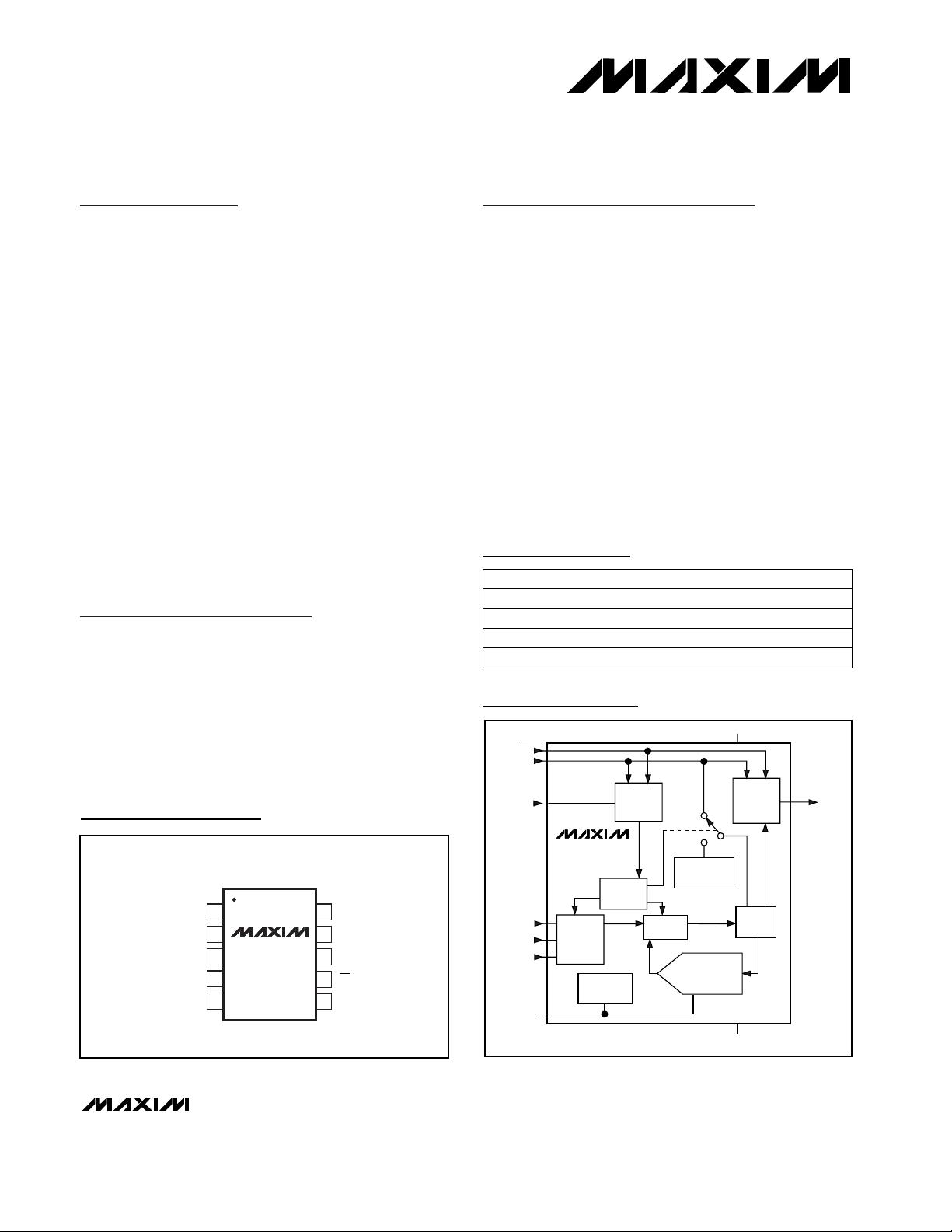
1
2
3
4
5
10
9
8
7
6
SCLK
DOUT
DIN
CSGND
CH1
CH0
V
DD
MAX1108
MAX1109
µMAX
TOP VIEW
COMREF
INPUT
SHIFT
REGISTER
CONTROL
LOGIC
T/H
SAR
INTERNAL
OSCILLATOR
OUTPUT
SHIFT
REGISTER
V
DD
ANALOG
INPUT
MUX
INTERNAL
REFERENCE
DOUT
SCLK
DIN
CH0
COM
REF
CH1
CS
GND
CHARGE
REDISTRIBUTION
DAC
MAX1108
MAX1109
Functional Diagram
19-1399; Rev 1; 6/03
Pin Configuration
Ordering Information
PART
MAX1108CUB
MAX1108EUB -40°C to +85°C
0°C to +70°C
TEMP RANGE PIN-PACKAGE
10 µMAX
10 µMAX
MAX1109CUB
MAX1109EUB -40°C to +85°C
0°C to +70°C 10 µMAX
10 µMAX
SPI and QSPI are trademarks of Motorola, Inc. MICROWIRE is a trademark of National Semiconductor Corp.
For pricing, delivery, and ordering information, please contact Maxim/Dallas Direct! at
1-888-629-4642, or visit Maxim’s website at www.maxim-ic.com.
MAX1108/MAX1109
Single-Supply, Low-Power,
2-Channel, Serial 8-Bit ADCs
2 _______________________________________________________________________________________
ABSOLUTE MAXIMUM RATINGS
ELECTRICAL CHARACTERISTICS—MAX1108
(V
DD
= +2.7V to +3.6V; unipolar input mode; COM = GND, f
SCLK
= 500kHz, external clock mode (50% duty cycle); 10 clocks/conver-
sion cycle (50ksps); 1µF capacitor at REF, external +2.048V reference at REF; T
A
= T
MIN
to T
MAX
; unless otherwise noted. Typical
values are at T
A
= +25°C.)
Stresses beyond those listed under “Absolute Maximum Ratings” may cause permanent damage to the device. These are stress ratings only, and functional
operation of the device at these or any other conditions beyond those indicated in the operational sections of the specifications is not implied. Exposure to
absolute maximum rating conditions for extended periods may affect device reliability.
V
DD
to GND..............................................................-0.3V to +6V
CH0, CH1, COM, REF, DOUT to GND .......-0.3V to (V
DD
+ 0.3V)
DIN, SCLK, CS to GND ............................................-0.3V to +6V
Continuous Power Dissipation (T
A
= +70°C)
10-pin µMAX (derate 5.6mW/°C above +70°C) ............444mW
Operating Temperature Ranges
MAX110_CUB ......................................................0°C to +70°C
MAX110_EUB ...................................................-40°C to +85°C
Storage Temperature Range .............................-65°C to +150°C
Lead Temperature (soldering, 10s) .................................+300°C
V
DD
= 2.7V to 3.6V
V
DD
= 5.5V (Note 2)
No missing codes over temperature
CONDITIONS
±0.15 ±0.5
bits8Resolution
LSB
±0.2
INLRelative Accuracy (Note 1)
LSB±1DNLDifferential Nonlinearity
UNITSMIN TYP MAXSYMBOLPARAMETER
V
DD
= 5.5V (Note 2)
V
DD
= 2.7V to 3.6V
LSB
±0.5
Offset Error
±0.2 ±1
LSB±1Gain Error (Note 3)
ppm/°C±0.8Gain Temperature Coefficient
T
A
= T
MIN
to T
MAX
T
A
= +25°C
mV50V
DD
/ 2 Sampling Accuracy
dB49SINADSignal-to-Noise Plus Distortion
dB-70THD
Total Harmonic Distortion
(up to the 5th harmonic)
LSB
±0.5
TUETotal Unadjusted Error
±1
LSB±0.1
Channel-to-Channel
Offset Matching
-3dB rolloff
Unipolar input, V
COM
= 0
MHz0.8Full-Power Bandwidth
MHz1.5BW
-3dB
Small-Signal Bandwidth
0V
REF
Input Voltage Range (Note 4)
dB68SFDRSpurious-Free Dynamic Range
Bipolar input, V
COM
or V
CH1
= V
REF
/ 2,
referenced to COM or CH1
V
±V
REF
/ 2
V
CH_
pF18C
IN
Input Capacitance
On/off-leakage current,
V
COM
or V
CH
= 0 or V
DD
µA±0.01 ±1Multiplexer Leakage Current
DC ACCURACY
DYNAMIC PERFORMANCE (10kHz sine-wave input, 2.048Vp-p, 50ksps, 500kHz external clock)
ANALOG INPUTS
µA
MAX1108/MAX1109
Single-Supply, Low-Power,
2-Channel, Serial 8-Bit ADCs
_______________________________________________________________________________________ 3
ELECTRICAL CHARACTERISTICS—MAX1108 (continued)
(V
DD
= +2.7V to +3.6V; unipolar input mode; COM = GND, f
SCLK
= 500kHz, external clock mode (50% duty cycle); 10 clocks/conver-
sion cycle (50ksps); 1µF capacitor at REF, external +2.048V reference at REF; T
A
= T
MIN
to T
MAX
; unless otherwise noted. Typical
values are at T
A
= +25°C.)
CONDITIONS UNITSMIN TYP MAXSYMBOLPARAMETER
External clock, 500kHz, 10 sclks/conv
Internal clock
External clock, 2MHz
µs
20
t
CONV
Conversion Time (Note 5)
35
µs1t
ACQ
Track/Hold Acquisition Time
ps<50Aperture Jitter
ns10Aperture Delay
kHz400Internal Clock Frequency
(Note 6)
0 to 0.5mA (Note 7)
ppm/°C±50REF Tempco
µA150I
REFSC
REF Short-Circuit Current
mV2.5Load Regulation
kHz50 500
V1.968 2.048 2.128V
REF
Output Voltage
+2.048V at REF, full scale,
500kHz external clock
µA120Input Current
V2.7 3 5.5V
DD
Supply Voltage
Power down, V
DD
= 2.7V to 3.6V (Note 9)
Full-scale input, V
DD
= 2.7V to 3.6V
0.5 2.5
I
DD
mV±0.4 ±4PSRPower-Supply Rejection (Note 10)
V
DD
= 2.7V to 3.6V,
C
L
= 10pF
V
DD
= 5.5V,
C
L
= 10pF
105 250
130
µF1Capacitive Bypass at REF
V0.2V
HYST
Input Hysteresis
V0.8V
IL
Threshold Voltage Low
µA±1I
IH
Input Current High
V
DD
≤ 3.6V
V
DD
> 3.6V
V2
V3
V
IH
Threshold Voltage High
MHz2
External Clock Frequency Range
V1.0 V
DD
+ 0.05Input Voltage Range
µA±1I
IL
Input Current Low
pF15C
IN
Input Capacitance
For data transfer only
Internal reference
External reference 70
Internal reference
External reference 95
µASupply Current (Notes 2, 8)
TRACK/HOLD
INTERNAL REFERENCE
EXTERNAL REFERENCE
POWER REQUIREMENTS
DIGITAL INPUTS (DIN, SCLK, and CS)
Wake-Up Time
MAX1108/MAX1109
Single-Supply, Low-Power,
2-Channel, Serial 8-Bit ADCs
4 _______________________________________________________________________________________
CS = V
DD
CS = V
DD
pF15C
OUT
Three-State Output Capacitance
µA±0.01 ±10I
L
Three-State Leakage Current
Figure 1, C
LOAD
= 100pF
Figure 1, C
LOAD
= 100pF
Figure 2, C
LOAD
= 100pF
ns240t
DV
CS Fall to Output Enable
ns
CONDITIONS
20 200t
DO
SCLK Fall to Output Data Valid
ns240t
TR
CS Rise to Output Disable
ns100t
DS
DIN to SCLK Setup Time
µs1.0t
ACQ
Acquisition Time
ns0t
DH
DIN to SCLK Hold Time
External reference
Internal reference (Note 11)
µs20
ns200t
CL
SCLK Pulse Width Low
ms12
t
WAKE
Wake-Up Time
ns0t
CSH
CS to SCLK Rise Hold
ns100t
CSS
CS to SCLK Rise Setup
ns200t
CH
SCLK Pulse Width High
UNITSMIN TYP MAXSYMBOLPARAMETER
I
SINK
= 5mA
I
SOURCE
= 0.5mA
I
SINK
= 16mA
V0.4
VV
DD
- 0.5V
OH
Output High Voltage
V0.8
V
OL
Output Low Voltage
ELECTRICAL CHARACTERISTICS—MAX1108 (continued)
(V
DD
= +2.7V to +3.6V; unipolar input mode; COM = GND, f
SCLK
= 500kHz, external clock mode (50% duty cycle); 10 clocks/conver-
sion cycle (50ksps); 1µF capacitor at REF, external +2.048V reference at REF; T
A
= T
MIN
to T
MAX
; unless otherwise noted. Typical
values are at T
A
= +25°C.)
ELECTRICAL CHARACTERISTICS—MAX1109
(V
DD
= +4.5V to +5.5V; unipolar input mode; COM = GND, f
SCLK
= 500kHz, external clock (50% duty cycle); 10 clocks/conversion
cycle (50ksps); 1µF capacitor at REF, external +4.096V reference at REF; T
A
= T
MIN
to T
MAX
; unless otherwise noted. Typical values
are at T
A
= +25°C.)
V
DD
= 4.5V to 5.5V LSBOffset Error ±0.2 ±1
LSB±1
V
DD
= 4.5V to 5.5V
No missing codes over temperature
Gain Error (Note 3)
ppm/°C±0.8
CONDITIONS
Gain Temperature Coefficient
T
A
= T
MIN
to T
MAX
T
A
= +25°C
mV50V
DD
/ 2 Sampling Accuracy
LSB
±0.5
TUETotal Unadjusted Error
±1
LSB±0.1
Channel-to-Channel
Offset Matching
±0.15 ±0.5
bits8Resolution
LSBINLRelative Accuracy (Note 1)
LSB±1DNLDifferential Nonlinearity
UNITSMIN TYP MAXSYMBOLPARAMETER
DIGITAL OUTPUT (DOUT)
TIMING CHARACTERISTICS (Figures 8, 9, and 10)
DC ACCURACY
MAX1108/MAX1109
Single-Supply, Low-Power,
2-Channel, Serial 8-Bit ADCs
_______________________________________________________________________________________ 5
ELECTRICAL CHARACTERISTICS—MAX1109 (continued)
(V
DD
= +4.5V to +5.5V; unipolar input mode; COM = GND, f
SCLK
= 500kHz, external clock (50% duty cycle); 10 clocks/conversion
cycle (50ksps); 1µF capacitor at REF, external +4.096V reference at REF; T
A
= T
MIN
to T
MAX
; unless otherwise noted. Typical values
are at T
A
= +25°C.)
ps<50Aperture Jitter
ns10Aperture Delay
kHz400Internal Clock Frequency
0 to 0.5mA (Note 7) ppm/°C±50REF Tempco
mA
CONDITIONS
5I
REFSC
REF Short-Circuit Current
mV2.5Load Regulation
kHz50 500
V
V3.936 4.096 4.256V
REF
Output Voltage
+4.096V at REF, full scale,
500kHz external clock
µA120Input Current
1.0 V
DD
+ 0.05Input Voltage Range
µF1Capacitive Bypass at REF
UNITSMIN TYP MAXSYMBOLPARAMETER
External clock, 2MHz
dBSINADSignal-to-Noise Plus Distortion 49
µs1t
ACQ
Track/Hold Acquisition Time
External clock, 500kHz, 10 sclks/conv
Internal clock
µs
20
t
CONV
Conversion Time (Note 5)
35
SFDRSpurious Free Dynamic Range dB
dB
68
THD
Total Harmonic Distortion
(up to the 5th harmonic)
-70
Full-Power Bandwidth MHz
Unipolar input, V
COM
= 0 0V
REF
-3dB rolloff MHz
0.8
BW
-3dB
Small-Signal Bandwidth 1.5
V
CH_
Input Voltage Range (Note 4) V
Multiplexer Leakage Current µA
On/off-leakage current,
V
CH
= 0 or V
DD
±0.01 ±1
pFC
IN
Input Capacitance 18
Bipolar input, V
COM
or V
CH1
= V
REF
/ 2,
referenced to COM or CH1
±V
REF
/ 2
MHz2
External Clock Frequency Range
DYNAMIC PERFORMANCE (10kHz sine-wave input, 4.096Vp-p, 50ksps, 500kHz external clock)
ANALOG INPUTS
TRACK/HOLD
EXTERNAL REFERENCE
INTERNAL REFERENCE
For data transfer only
剩余20页未读,继续阅读
资源评论
芯脉芯城
- 粉丝: 3
- 资源: 4031
上传资源 快速赚钱
- 我的内容管理 展开
- 我的资源 快来上传第一个资源
- 我的收益 登录查看自己的收益
- 我的积分 登录查看自己的积分
- 我的C币 登录后查看C币余额
- 我的收藏
- 我的下载
- 下载帮助
安全验证
文档复制为VIP权益,开通VIP直接复制
信息提交成功