MAX163BCWG maxim 美信芯片 电子元器件中文版规格手册.pdf
需积分: 5 166 浏览量
2023-06-06
10:21:08
上传
评论
收藏 983KB PDF 举报


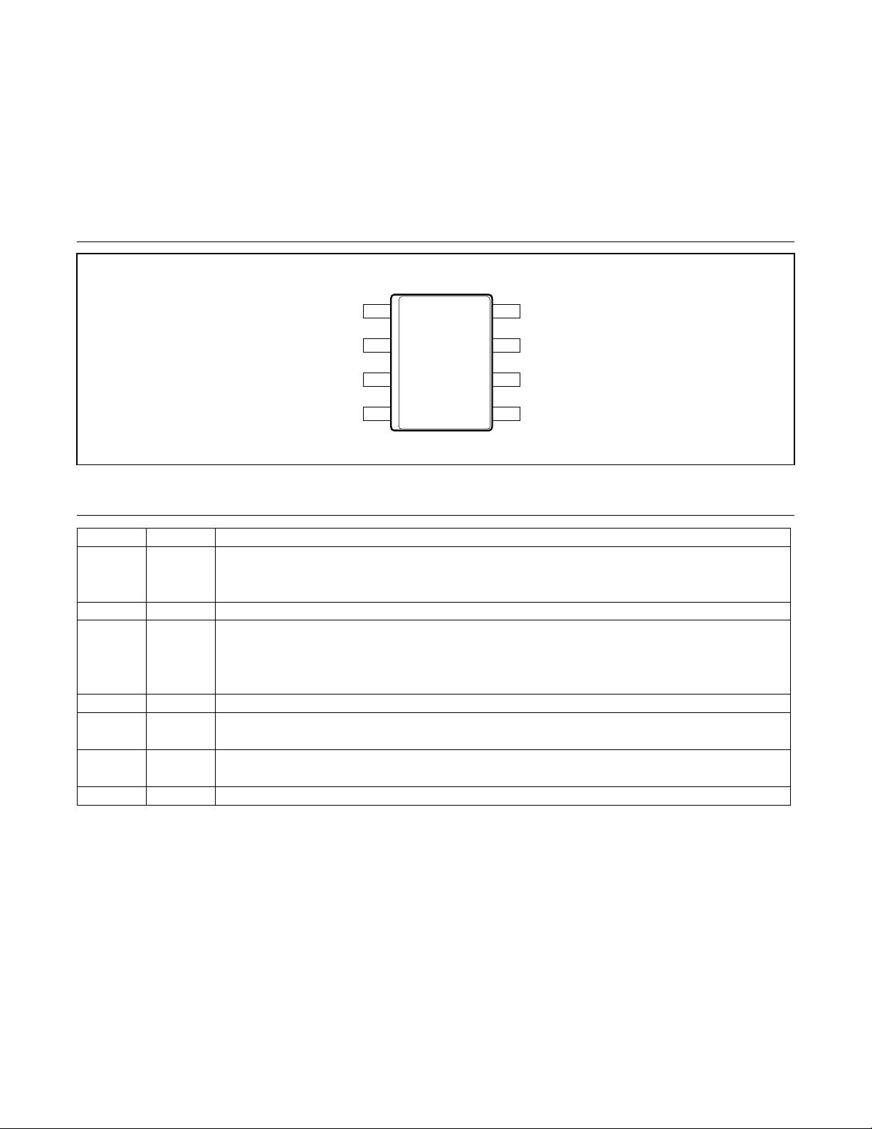
DS1683
Total-Elapsed-Time and Event Recorder with Alarm
General Description
The DS1683 is an integrated elapsed-time recorder con-
taining a factory-calibrated, low-temperature-coefficient
RC time base that eliminates the need for an external
crystal. Using EEPROM technology to maintain data in
the absence of power, the DS1683 requires no backup
power source. The DS1683 detects and records the num-
ber of falling edge transitions on the EVENT pin as well
as the total cumulative time that the EVENT pin is held
high. The ALARM pin alerts the user when the total time
accumulated equals or exceeds the user-programmed
alarm value, or when the total number of events equals
or exceeds the user-programmed alarm value. The polar-
ity of the open-drain ALARM pin can be programmed
to either drive low or become high impedance upon an
alarm condition. The DS1683 is ideal for applications that
monitor the total amount of time that a device has been
in operation and/or the number of uses since inception
service, repair, or last calibration.
Applications
High-Temp, Rugged, Industrial Applications Where
Vibration or Shock Could Damage a Quartz Crystal
Any System Where Time-of-Use is Important to
Track
Power-on-Time Recorder
Benefits and Features
S Records the Total Time the EVENT Input Has Been
Active High and Number of Events (Falling Edges
of EVENT) That Have Occurred
S 32-Bit, Nonvolatile, Elapsed Time Counter (ETC)
Monitors Event Duration with Quarter Seconds
Resolution and Provides 34 Years of Total Time
Accumulation
S Nonvolatile 16-Bit Event Counter Records the
Number of Falling Edges Seen by the EVENT Pin
S Calibrated, Low-Temperature-Coefficient RC Time
Base
S 16 Bytes of User EEPROM
S Password Protection Scheme (4 Bytes)
S I
2
C-Compatible Interface
S +2.5V to +5.5V Operating Voltage Range
19-6388; Rev 0; 6/12
Ordering Information appears at end of data sheet.
For related parts and recommended products to use with this part,
refer to www.maximintegrated.com/DS1683.related.
For pricing, delivery, and ordering information, please contact Maxim Direct at
1-888-629-4642, or visit Maxim Integrated’s website at www.maximintegrated.com.


剩余21页未读,继续阅读
资源评论


