TI-DS125MB203.pdf
86 浏览量
2022-12-16
22:54:34
上传
评论 4
收藏 1.48MB PDF 举报

DRIVE 1
EXPANDER
MB203
S_INA0
S_OUTA1
D_IN0
RXA_1
TX
RX
SEL0
SEL1
EXPANDER
TX
RX
D_IN1
S_OUTB1
S_INB0
S_INA1
S_INA1
S_OUTA0
S_OUTB0
D_OUT0
D_OUT1
RXA_0
TXA_1
TXA_0
RXB_1
RXB_0
TXB_1
TXB_0
DRIVE 0
VDD (2.5 V)
D_IN+
D_IN-
AD0
AD1
AD2
AD3
ENSMB
SCL
(2)
READ_EN / SEL1
SDA
(2)
S_OUTA+
S_OUTA-
GND (DAP)
(1) Schematic shows connection for SMBus Slave Mode (ENSMB = 1 k: to VIN)
For SMBus Master Mode or Pin Mode configuration, the connections are different.
(2) SMBus signals must be pulled up elsewhere in the system.
(3) Schematic requires different connections for 2.5 V mode.
(4) Schematic requires pullup resistor for 10G-KR Mode.
VIN
0.1F
(x5)
SMBus Slave
Mode
(1)
S_OUTB+
S_OUTB-
VDD_SEL
VIN (3.3 V)
D_OUT+
D_OUT-
S_INA+
S_INA-
S_INB+
S_INB-
Address straps
(pull-up to VIN or
pull-down to
GND)
(1)
1F
3.3V
(3)
10F
ALL_DONE
MODE
To SMBus/I2C
Host Controller
MB203
SMBus Slave Mode
(1)
SMBus Slave Mode
(1)
SATA/SAS
Mode
(4)
GND
RESET
1 OF 2
SEL0
SMBus Slave Mode
(1)
INPUT_EN
Product
Folder
Sample &
Buy
Technical
Documents
Tools &
Software
Support &
Community
An IMPORTANT NOTICE at the end of this data sheet addresses availability, warranty, changes, use in safety-critical applications,
intellectual property matters and other important disclaimers. PRODUCTION DATA.
English Data Sheet: SNLS432
DS125MB203
ZHCSEN5C –OCTOBER 2012–REVISED DECEMBER 2015
DS125MB203 具具有有均均衡衡和和去去加加重重功功能能的的低低功功耗耗 12.5Gbps 双双通通道道
2:1/1:2 复复用用器器/缓缓冲冲器器
1
1 特特性性
1
• 12.5Gbps 双通道 2:1 复用器,1:2 开关或扇出
• 低至 390mW 的总功耗(典型值)
• 高级信号调节 功能:
– 频率为 6.25GHz 时,最高可支持 30dB 的接收
均衡功能
– 发送去加重功能高达 –12dB
– 发送输出电压控制:600mV 至 1300mV
• 可通过引脚选择、电可擦可编程只读存储器
(EEPROM) 或 SMBus 接口进行编程
• 2.5V 或 3.3V 可选电源电压
• 运行温度范围:–40°C 至 +85°C
2 应应用用
• 10GE,10G-KR
• PCIe 1 代/2 代/3 代
• SAS2/SATA3(最高可达 6Gbps)
• XAUI,RXAUI
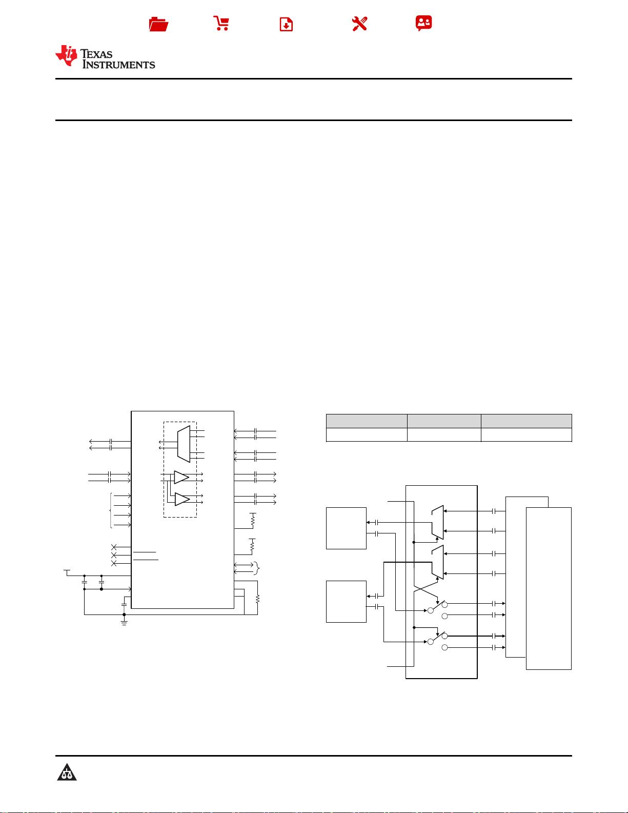
简简化化功功能能框框图图
3 说说明明
DS125MB203 器件是一款具有信号调节功能的双端口
2:1 复用器和 1:2 开关或扇出缓冲器,适用于数据传输
速率最高可达 12.5Gbps 的 10GE、10G-KR
(802.3ap)、光纤通道、PCIe、无线带宽、
SATA3/SAS2 和 其他高速总线 应用。接收器的连续时
间线性均衡器 (CTLE) 可提供必要的升压性能,从而在
12.5Gbps 的速率下对长达 30 英寸的 FR-4 或 8M 电
缆 (AWG-24) 进行补偿。该片上特性免除了对外部信
号调节器的需求。发送器 具有 可编程幅值电压等级,
可在 600 mVp-p 至 1300 mVp-p 范围内进行选择,同
时实现高达 12dB 的去加重。
DS125MB203 可配置为支持 PCIe、SAS/SATA、
10G-KR 或其他信号传输协议。在 10G-KR 和 PCIe 3
代模式下运行时,DS125MB203 以透明方式允许主机
控制器和端点优化完整链路并协商发送均衡器系数。这
种链路协商协议的无缝管理可确保系统级互操作性并最
大限度地降低延迟。
器器件件信信息息
(1)
器器件件型型号号 封封装装 封封装装尺尺寸寸((标标称称值值))
DS125MB203 WQFN (54) 10.00mm x 5.50mm
(1) 要了解所有可用封装,请见数据表末尾的可订购产品附录。
典典型型应应用用


剩余53页未读,继续阅读
资源评论


