没有合适的资源?快使用搜索试试~ 我知道了~
TI-CC115L.pdf
5星 · 超过95%的资源 需积分: 10 1 下载量 130 浏览量
2022-12-16
21:15:36
上传
评论 4
收藏 1.66MB PDF 举报
温馨提示
试读
72页
TI-CC115L.pdf
资源推荐
资源详情
资源评论
Product
Folder
Sample &
Buy
Technical
Documents
Tools &
Software
Support &
Community
CC115L
SWRS105B –MAY 2011–REVISED JUNE 2014
CC115L Value Line Transmitter
1 Device Overview
1.1 Features
1
• RF Performance • General
– Programmable Output Power up to +12 dBm – Few External Components; Fully Integrated
Frequency Synthesizer
– Programmable Data Rate from 0.6 to 600 kbps
– Green Package: RoHS Compliant and No
– Frequency Bands: 300–348 MHz,
Antimony or Bromine
387–464 MHz, and 779–928 MHz
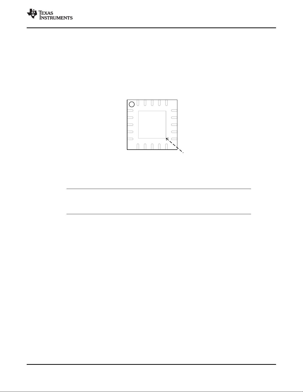
– Small Size (QLP 4- x 4-mm Package, 20 Pins)
– 2-FSK, 4-FSK, GFSK, and OOK Supported
– Suited for Systems Targeting Compliance with
• Digital Features
EN 300 220 V2.3.1 (Europe) and FCC CFR Part
– Flexible Support for Packet Oriented Systems
15 (US)
– On-chip Support for Sync Word Insertion,
– Support for Asynchronous and Synchronous
Flexible Packet Length, and Automatic CRC
Serial Transmit Mode for Backward
Calculation
Compatibility with Existing Radio
• Low-Power Features
Communication Protocols
– 200-nA Sleep Mode Current Consumption
– Fast Startup Time; 240 μs From Sleep to TX
Mode
– 64-Byte TX FIFO
1.2 Applications
• Ultra Low-Power Wireless Applications Operating • Remote Controls
in the 315-, 433-, 868-, 915-MHz ISM or SRD
• Toys
Bands
• Home and Building Automation
• Wireless Alarm and Security Systems
• Active RFID
• Industrial Monitoring and Control
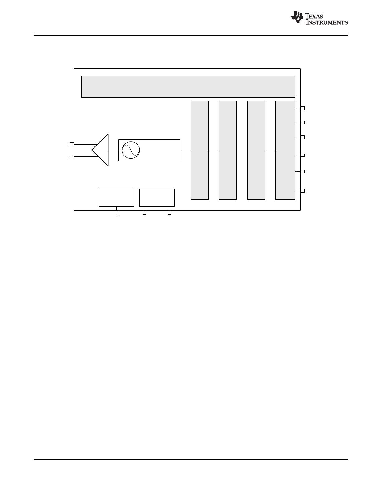
1.3 Description
The CC115L is a cost optimized sub-1 GHz RF transmitter. The circuit is based on the popular CC1101
RF transceiver, and RF performance characteristics are identical. The CC115L value line transmitter
together with the CC113L value line receiver enables a low-cost RF link.
The RF transmitter is integrated with a highly configurable baseband modulator. The modem supports
various modulation formats and has a configurable data rates from 0.6 to 600 kbps.
The CC115L provides extensive hardware support for packet handling, data buffering, and burst
transmissions.
The main operating parameters and the 64-byte transmit FIFO of CC115L can be controlled through a
serial peripheral interface (SPI). In a typical system, the CC115L will be used together with a
microcontroller and a few additional passive components.
Device Information
(1)
PART NUMBER PACKAGE BODY SIZE
CC115LRGP QFN (20) 4.00 mm × 4.00 mm
(1) For more information on these devices, see Section 8, Mechanical Packaging and Orderable
Information.
1
An IMPORTANT NOTICE at the end of this data sheet addresses availability, warranty, changes, use in safety-critical applications,
intellectual property matters and other important disclaimers. PRODUCTION DATA.
BIAS
PA
RBIAS
XOSC_Q1
CSn
SI
SO (GDO1)
XOSC
SCLK
FREQ
SYNTH
Packet Handler
Modulator
TX FIFO
Digital Interface to MCU
Radio Control
GDO0
RF_P
RF_N
GDO2
XOSC_Q2
CC115L
SWRS105B –MAY 2011–REVISED JUNE 2014
www.ti.com
1.4 Functional Block Diagram
Figure 1-1 shows a functional block diagram of the device.
Figure 1-1. Functional Block Diagram
2 Device Overview Copyright © 2011–2014, Texas Instruments Incorporated
Submit Documentation Feedback
Product Folder Links: CC115L
CC115L
www.ti.com
SWRS105B –MAY 2011–REVISED JUNE 2014
Table of Contents
1 Device Overview ......................................... 1 5.9 Modulation Formats ................................. 26
1.1 Features .............................................. 1 5.10 Radio Control........................................ 27
1.2 Applications........................................... 1 5.11 TX FIFO ............................................. 32
1.3 Description............................................ 1 5.12 Frequency Programming............................ 34
1.4 Functional Block Diagram ............................ 2 5.13 VCO ................................................. 35
2 Revision History ......................................... 4 5.14 Voltage Regulators.................................. 35
3 Terminal Configuration and Functions.............. 5 5.15 Output Power Programming ........................ 36
3.1 Pin Diagram .......................................... 5 5.16 General Purpose and Test Output Control Pins .... 38
3.2 Signal Descriptions ................................... 6 5.17 Asynchronous and Synchronous Serial Operation.. 40
4 Specifications ............................................ 7 5.18 System Considerations and Guidelines ............. 41
4.1 Absolute Maximum Ratings .......................... 7 5.19 Configuration Registers ............................. 43
4.2 Handling Ratings ..................................... 7 5.20 Development Kit Ordering Information.............. 57
4.3 Recommended Operating Conditions ................ 7 6 Applications, Implementation, and Layout........ 58
4.4 General Characteristics .............................. 7 6.1 Bias Resistor ........................................ 58
4.5 Current Consumption ................................. 8 6.2 Balun and RF Matching ............................. 58
4.6 RF Transmit Section.................................. 9 6.3 Crystal ............................................... 60
4.7 Crystal Oscillator .................................... 11 6.4 Reference Signal.................................... 60
4.8 Frequency Synthesizer Characteristics ............. 11 6.5 Additional Filtering .................................. 60
4.9 DC Characteristics .................................. 11 6.6 Power Supply Decoupling........................... 60
4.10 Power-On Reset .................................... 12 6.7 PCB Layout Recommendations..................... 61
4.11 Thermal Characteristics ............................. 12 7 Device and Documentation Support ............... 62
5 Detailed Description ................................... 13 7.1 Device Support ...................................... 62
5.1 Overview ............................................ 13 7.2 Documentation Support ............................. 63
5.2 Functional Block Diagram........................... 13 7.3 Trademarks.......................................... 63
5.3 Configuration Overview ............................. 14 7.4 Electrostatic Discharge Caution..................... 64
5.4 Configuration Software.............................. 16 7.5 Export Control Notice ............................... 64
5.5 4-wire Serial Configuration and Data Interface ..... 17 7.6 Glossary............................................. 64
5.6 Microcontroller Interface and Pin Configuration..... 21 7.7 Additional Acronyms ................................ 64
5.7 Data Rate Programming ............................ 22 8 Mechanical Packaging and Orderable
Information .............................................. 66
5.8 Packet Handling Hardware Support................. 23
8.1 Packaging Information .............................. 66
Copyright © 2011–2014, Texas Instruments Incorporated Table of Contents 3
Submit Documentation Feedback
Product Folder Links: CC115L
CC115L
SWRS105B –MAY 2011–REVISED JUNE 2014
www.ti.com
2 Revision History
NOTE: Page numbers for previous revisions may differ from page numbers in the current version.
Changes from Revision A (September 2011) to Revision B Page
• Changed format of data sheet to standard TI format. ........................................................................... 1
• Changed reset value from 0x09 to 0x19 ......................................................................................... 55
• Changed the package designator from RTK to RGP .......................................................................... 66
4 Revision History Copyright © 2011–2014, Texas Instruments Incorporated
Submit Documentation Feedback
Product Folder Links: CC115L
1
20 19 18 17 16
15
14
13
12
11
109876
5
4
3
2
GND
Exposed die
attach pad
SCLK
SO (GDO1)
GDO2
DVDD
DCOUPL
GDO0
XOSC_Q1
AVDD
XOSC_Q2
AVDD
RF_P
RF_N
GND
AVDD
RBIAS
DGUARD
GND
SI
CSn
AVDD
CC115L
www.ti.com
SWRS105B –MAY 2011–REVISED JUNE 2014
3 Terminal Configuration and Functions
3.1 Pin Diagram
The CC115L pinout is shown in Figure 3-1 and Table 3-1. See Section 5.16 for details on the I/O
configuration.
Figure 3-1. Pinout Top View
NOTE
The exposed die attach pad must be connected to a solid ground plane as this is the main
ground connection for the chip.
Copyright © 2011–2014, Texas Instruments Incorporated Terminal Configuration and Functions 5
Submit Documentation Feedback
Product Folder Links: CC115L
剩余71页未读,继续阅读
资源评论
- m0_745259962023-02-01#完美解决问题 #运行顺畅 #内容详尽 #全网独家 #注释完整
不觉明了
- 粉丝: 3103
- 资源: 5330
上传资源 快速赚钱
- 我的内容管理 展开
- 我的资源 快来上传第一个资源
- 我的收益 登录查看自己的收益
- 我的积分 登录查看自己的积分
- 我的C币 登录后查看C币余额
- 我的收藏
- 我的下载
- 下载帮助
安全验证
文档复制为VIP权益,开通VIP直接复制
信息提交成功