没有合适的资源?快使用搜索试试~ 我知道了~
TI-TLV320AIC3104.pdf
需积分: 5 2 下载量 176 浏览量
2022-12-03
23:46:01
上传
评论 4
收藏 3.82MB PDF 举报
温馨提示
试读
104页
TI-TLV320AIC3104.pdf
资源推荐
资源详情
资源评论
用于便携式音频和电话的 TLV320AIC3104 低功耗立体声音频编解码器
1 特性
• 立体声音频 DAC:
– 102dBA 信噪比
– 16 位、20 位、24 位和 32 位数据
– 支持 8kHz 至 96kHz 的采样率
– 3D、低音、高音、EQ 或去加重效果
– 提供灵活的节能模式和性能
• 立体声音频 ADC:
– 92dBA 信噪比
– 支持 8kHz 至 96kHz 的采样率
– 在录音期间提供数字信号处理和噪声滤除功能
• 六个音频输入引脚:
– 一对立体声单端输入
– 一对立体声全差分输入
• 六个音频输出驱动器:
– 立体声全差动或单端耳机驱动器
– 全差动立体声线路输出
• 低功耗:3.3V 模拟电源电压、14mW 立体声、
48kHz 回放
• 具有无源模拟旁路的超低功耗模式
• 可编程 I/O 模拟增益
• 用于录音的自动增益控制 (AGC)
• 可编程麦克风偏置电平
• 用于灵活时钟生成的可编程 PLL
• I
2
C 控制总线
• 音频串行数据总线支持 I
2
S、左平衡和右平衡、
DSP 和 TDM 模式
• 广泛的模块化电源控制
• 电源:
– 模拟:2.7V 至 3.6V
– 数字内核:1.525V 至 1.95V
– 数字 I/O:1.1V 至 3.6V
• 封装:5mm × 5mm,32 引脚 VQFN
2 应用
• 耳机
• IP 网络摄像头
• IP 电话
• 无线扬声器
3 说明
TLV320AIC3104 是一款低功耗立体声音频编解码器,
具有立体声耳机放大器以及在单端或全差分配置下可编
程的多个输入和输出。该器件包括基于寄存器的全面电
源控制,可实现立体声 48kHz DAC 回放,在 3.3V 模
拟电源电压下的功耗低至 14mW,因此非常适合便携
式电池供电类音频和电话应用。
TLV320AIC3104 的录音路径包含集成式麦克风偏置、
数控立体声麦克风前置放大器和自动增益控制
(AGC),并在多个模拟输入中提供混频器/多路复用器
功能。在录音过程中,可编程滤波器能够滤除在数码相
机光学变焦期间可能产生的可闻噪声。回放路径包括混
频器/多路复用器功能(从立体声 DAC 和所选输入,经
可编程音量控制至各种输出)。
器件信息
(1)
器件型号 封装
封装尺寸(标称值)
TLV320AIC3104 VQFN (32) 5.00mm × 5.00mm
(1) 如需了解所有可用封装,请参阅数据表末尾的可订购产品附
录。
简化版图表
TLV320AIC3104
ZHCSNE2G – MARCH 2007 – REVISED FEBRUARY 2021
本文档旨在为方便起见,提供有关 TI 产品中文版本的信息,以确认产品的概要。有关适用的官方英文版本的最新信息,请访问
www.ti.com,其内容始终优先。TI 不保证翻译的准确性和有效性。在实际设计之前,请务必参考最新版本的英文版本。
English Data Sheet: SLAS510
Table of Contents
1 特性................................................................................... 1
2 应用................................................................................... 1
3 说明................................................................................... 1
4 Revision History.............................................................. 2
5 Description (Continued)..................................................4
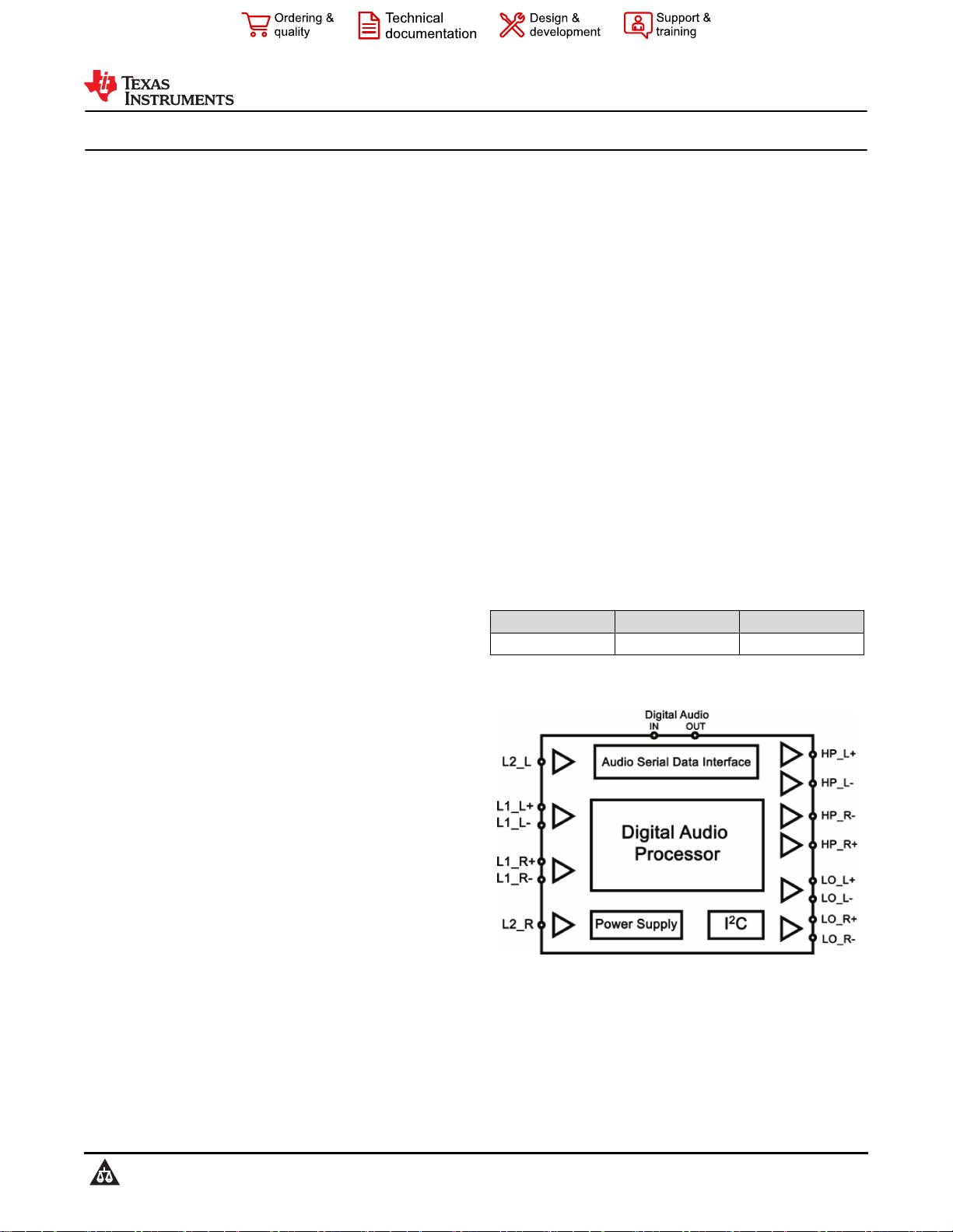
6 Device Comparison Table............................................... 4
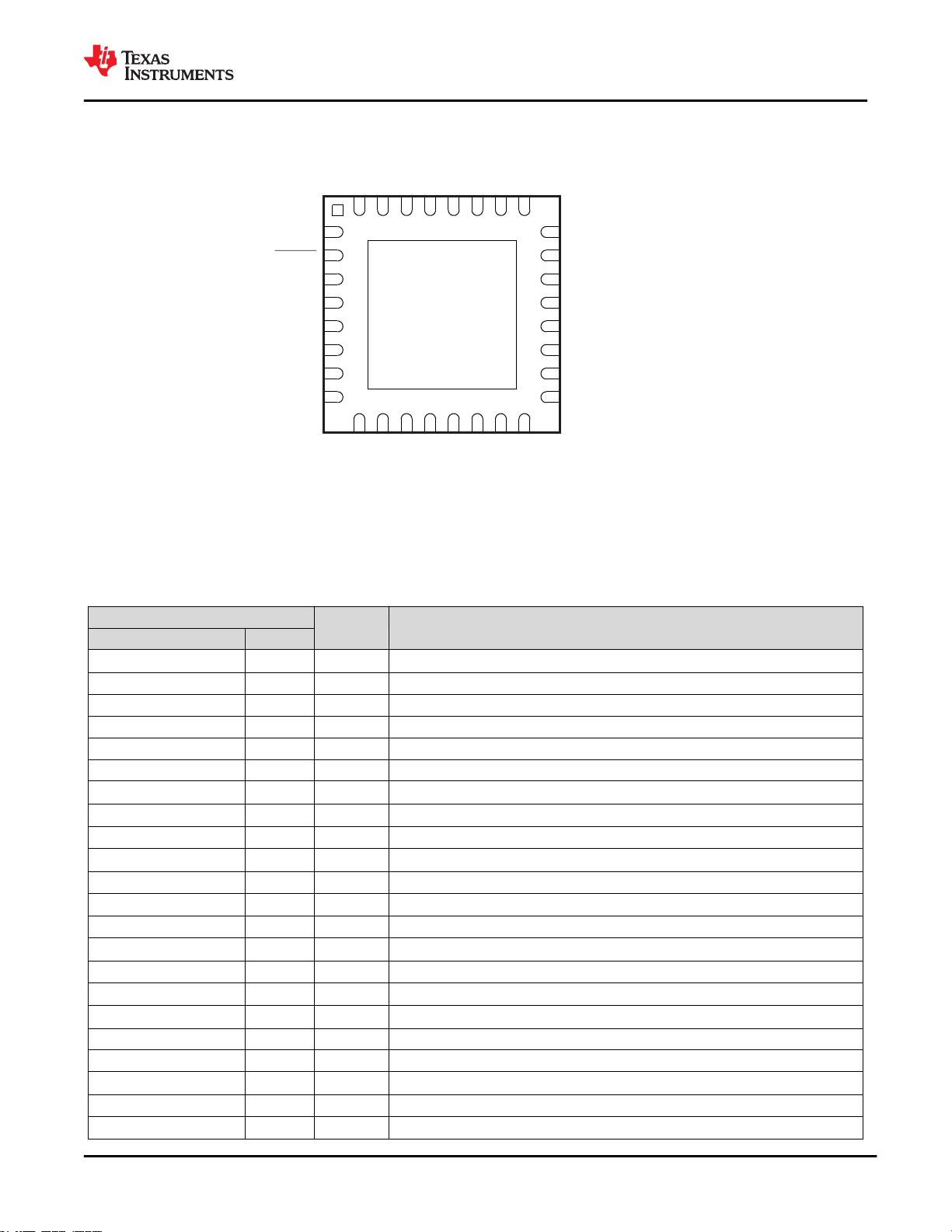
7 Pin Configuration and Functions...................................5
8 Specifications.................................................................. 7
8.1 Absolute Maximum Ratings........................................ 7
8.2 ESD Ratings............................................................... 7
8.3 Recommended Operating Conditions.........................7
8.4 Thermal Information....................................................8
8.5 Electrical Characteristics.............................................8
8.6 Audio Data Serial Interface Timing Requirements....13
8.7 Timing Diagrams.......................................................14
8.8 Typical Characteristics.............................................. 17
9 Parameter Measurement Information.......................... 19
10 Detailed Description....................................................19
10.1 Overview................................................................. 19
10.2 Functional Block Diagrams..................................... 20
10.3 Feature Description.................................................22
10.4 Device Functional Modes........................................43
10.5 Programming.......................................................... 45
10.6 Register Maps.........................................................48
11 Application and Implementation................................ 89
11.1 Application Information............................................89
11.2 Typical Applications.................................................89
12 Power Supply Recommendations..............................92
13 Layout...........................................................................93
13.1 Layout Guidelines................................................... 93
13.2 Layout Example...................................................... 94
14 Device and Documentation Support..........................95
14.1 接收文档更新通知................................................... 95
14.2 支持资源..................................................................95
14.3 Trademarks.............................................................95
14.4 静电放电警告.......................................................... 95
14.5 术语表..................................................................... 95
4 Revision History
Changes from Revision F (December 2016) to Revision G (February 2021) Page
•
更新了整个文档的表、图和交叉参考的编号格式
............................................................................................... 1
• 通篇将 QFN 更改为 VQFN..................................................................................................................................1
• 更改了
应用
部分..................................................................................................................................................1
• Changed Device Comparison Table: changed title, added TLV320AIC3109-Q1 row.........................................4
• Deleted System Thermal Characteristics table...................................................................................................8
• Added input impedance parameter in Electrical Characteristics table: added single-ended to test conditions of
first two rows, added last two rows to parameter................................................................................................8
• Deleted current consumption parameter, Stereo line in to stereo line out , no signal test condition.................. 8
• Changed list of intended applications in Overview section...............................................................................19
• Added Functional Block Diagram With Registers figure and added caption to Functional Block Diagram figure
..........................................................................................................................................................................20
• Added note to Audio Clock Generation section................................................................................................ 26
• Changed 2 MHz to 512 kHz in 512 kHz
≤
(PLLCLK_IN/P)
≤
20 MHz PLL example in Audio Clock
Generation section............................................................................................................................................26
• Added Left Channel Signal Path and Right Channel Signal Path figures to Audio Analog Inputs section....... 35
• Deleted Analog Input Bypass Path Functionality section................................................................................. 43
• Changed Passive Analog Bypass Mode Configuration figure to remove LINE 2L/R input bypass ................. 43
• Added reset value to D0 row in Page 0, Register 9: Audio Serial Data Interface Control Register B table......48
• Changed D3–D0 row reset value from 000 to 0000 in Page 0, Register 37: DAC Power and Output Driver
Control Register table....................................................................................................................................... 48
• Changed reset value from 1 to 0 and changed description of bit D1 in Page 0, Register 51: HPLOUT Output
Level Control Register ..................................................................................................................................... 65
• Changed reset value from 1 to 0 and changed description of bit D1 in Page 0, Register 58: HPLCOM Output
Level Control Register ..................................................................................................................................... 65
• Changed reset value from 1 to 0 and changed description of bit D1 in Page 0, Register 65: HPROUT Output
Level Control Register ..................................................................................................................................... 65
• Changed reset value from 1 to 0 and changed description of bit D1 in Page 0, Register 72: HPRCOM Output
Level Control Register ..................................................................................................................................... 65
TLV320AIC3104
ZHCSNE2G – MARCH 2007 – REVISED FEBRUARY 2021
www.ti.com.cn
2
Submit Document Feedback
Copyright © 2021 Texas Instruments Incorporated
Product Folder Links: TLV320AIC3104
• Changed reset value from 1 to 0 and changed description of bit D1 in Page 0, Register 86: LEFT_LOP/M
Output Level Control Register ......................................................................................................................... 65
• Changed Read/Write value from R to R/W in bit D0 of Page 0, Register 86: LEFT_LOP/M Output Level
Control Register ...............................................................................................................................................65
• Changed reset value from 1 to 0 and changed description of bit D1 in Page 0, Register 93: RIGHT_LOP/M
Output Level Control Register ......................................................................................................................... 65
• Changed Read/Write value from R to R/W in bit D0 of Page 0, Register 93: RIGHT_LOP/M Output Level
Control Register ...............................................................................................................................................65
• Changed Read/Write value from R to R/W in bit D0 of Page 0, Register 96: Sticky Interrupt Flags Register ....
65
• Changed reset value from 00 to 11 and changed description of bits D5–D4 in Page 0, Register 107: New
Programmable ADC Digital Path and I
2
C Bus Condition Register .................................................................. 65
• Changed description of bits D6 and D2 in Page 0, Register 108: Passive Analog Signal Bypass Selection
During Power Down Register .......................................................................................................................... 65
• Changed Cell Phone to Portable in title of Typical Connections With Headphone and External Speaker Driver
in Portable Application section and in title of Typical Connections With Headphone and External Speaker
Driver in Portable Applications figure................................................................................................................89
Changes from Revision E (November 2016) to Revision F (December 2016) Page
• Deleted paragraph "Another programmable option..." from the Input Impedance and VCM Control section...41
www.ti.com.cn
TLV320AIC3104
ZHCSNE2G – MARCH 2007 – REVISED FEBRUARY 2021
Copyright © 2021 Texas Instruments Incorporated
Submit Document Feedback
3
Product Folder Links: TLV320AIC3104
5 Description (Continued)
The TLV320AIC3104 contains four high-power output drivers as well as two fully differential output drivers. The
high-power output drivers can drive a variety of load configurations, including up to four channels of single-
ended 16-Ω headphones using AC-coupling capacitors, or stereo 16-Ω headphones in a capacitor-free output
configuration.
The stereo audio DAC supports sampling rates from 8 kHz to 96 kHz and includes programmable digital filtering
in the DAC path for 3D, bass, treble, midrange effects, speaker equalization, and de-emphasis for 32-kHz,
44.1-kHz, and 48-kHz sample rates. The stereo audio ADC supports sampling rates from 8 kHz to 96 kHz and is
preceded by programmable gain amplifiers or AGC that can provide up to 59.5-dB analog gain for low-level
microphone inputs. The TLV320AIC3104 provides an extremely high range of programmability for both attack
(8–1,408 ms) and for decay (0.05–22.4 seconds). This extended AGC range allows the AGC to be tuned for
many types of applications.
For battery-saving applications where neither analog nor digital signal processing are required, the device can
be put in a special analog signal passthrough mode. This mode significantly reduces power consumption, as
most of the device is powered down during this passthrough operation.
The serial control bus supports the I
2
C protocol, whereas the serial audio data bus is programmable for I2S, left-
and right-justified, DSP, or TDM modes. A highly programmable PLL is included for flexible clock generation and
support for all standard audio rates from a wide range of available MCLKs, varying from 512 kHz to 50 MHz, with
special attention paid to the most-popular cases of 12-MHz, 13-MHz, 16-MHz, 19.2-MHz, and 19.68-MHz
system clocks.
The TLV320AIC3104 operates from an analog supply of 2.7 V to 3.6 V, a digital core supply of 1.525 V to 1.95 V,
and a digital I/O supply of 1.1 V to 3.6 V. The device is available in a 5-mm × 5-mm 32-pin VQFN package.
6 Device Comparison Table
DEVICE NAME
DESCRIPTION
TLV320AIC3104 Low-power stereo CODEC with 6 inputs, 6 outputs, HP amplifier and enhanced digital effects
TLV320AIC3101 Same as TLV320AIC3104, but with speaker and HP amplifier
TLV320AIC3105 Same as TLV320AIC3104, but with all inputs single-ended
TLV320AIC3106 Same as TLV320AIC3104, but with 10 inputs and 7 outputs
TLV320AIC3107 Same as TLV320AIC3104, but with 7 inputs, 6 outputs and integrated mono class-D amplifier
TLV320AIC3109-Q1 Same as TLV320AIC3104, but AEC-Q100 qualified with 2 inputs, 6 outputs, and mono ADC and DAC
TLV320AIC3104
ZHCSNE2G – MARCH 2007 – REVISED FEBRUARY 2021
www.ti.com.cn
4
Submit Document Feedback
Copyright © 2021 Texas Instruments Incorporated
Product Folder Links: TLV320AIC3104
7 Pin Configuration and Functions
P0048-01
SDADVDD
DRVDD
MCLK
1
24
2
23
3
22
4
21
5
20
6
19
7
18
8
17
9
32
10
31
11
30
12
29
13
28
1427
1526
1625
MIC1LP/LINE1LP
BCLK
MIC1LM/LINE1LM
WCLK
MIC1RP/LINE1RP
DIN
MIC1RM/LINE1RM
DOUT
MIC2L/LINE2L/MICDET
DVSS
MICBIAS
IOVDD
MIC2R/LINE2R
SCL
RESET
HPROUT
RIGHT_LOM
HPRCOM
RIGHT_LOP
DRVSS
LEFT_LOM
HPLCOM
LEFT_LOP
HPLOUT
AVSS2
DRVDD
AVDD
AVSS1
NOTE: Connect device thermal pad to DRVSS.
图 7-1. RHB Package, 32-Pin (VQFN), Bottom View
表 7-1. Pin Functions
PIN
I/O DESCRIPTION
NAME NO.
AVDD 25
—
Analog DAC voltage supply, 2.7 V–3.6 V
AVSS1 17
—
Analog ADC ground supply, 0 V
AVSS2 26
—
Analog DAC ground supply, 0 V
BCLK 2 I/O Audio serial data bus bit clock input/output
DIN 4 I Audio serial data bus data input
DOUT 5 O Audio serial data bus data output
DRVDD 18
—
Analog ADC and output driver voltage supply, 2.7 V–3.6 V
DRVDD 24
—
Analog output driver voltage supply, 2.7 V–3.6 V
DRVSS 21
—
Analog output driver ground supply, 0 V
DVDD 32
—
Digital core voltage supply, 1.525 V–1.95 V
DVSS 6
—
Digital core, I/O ground supply, 0 V
HPLCOM 20 O
High-power output driver (left – or multi-functional)
HPLOUT 19 O High-power output driver (left +)
HPRCOM 22 O
High-power output driver (right – or multi-functional)
HPROUT 23 O High-power output driver (right +)
IOVDD 7
—
Digital I/O voltage supply, 1.1 V–3.6 V
LEFT_LOM 28 O
Left line output (–)
LEFT_LOP 27 O Left line output (+)
MCLK 1 I Master clock input
MIC1LM/LINE1LM 11 I
Left input – (diff only)
MIC1LP/LINE1LP 10 I Left input 1 (SE) or left input + (diff)
MIC1RM/LINE1RM 13 I
Right input – (diff only)
www.ti.com.cn
TLV320AIC3104
ZHCSNE2G – MARCH 2007 – REVISED FEBRUARY 2021
Copyright © 2021 Texas Instruments Incorporated
Submit Document Feedback
5
Product Folder Links: TLV320AIC3104
剩余103页未读,继续阅读
资源评论
不觉明了
- 粉丝: 3188
- 资源: 5486
上传资源 快速赚钱
- 我的内容管理 展开
- 我的资源 快来上传第一个资源
- 我的收益 登录查看自己的收益
- 我的积分 登录查看自己的积分
- 我的C币 登录后查看C币余额
- 我的收藏
- 我的下载
- 下载帮助
安全验证
文档复制为VIP权益,开通VIP直接复制
信息提交成功