没有合适的资源?快使用搜索试试~ 我知道了~
TI-TLV320AIC3100.pdf
需积分: 5 0 下载量 162 浏览量
2022-12-03
23:46:19
上传
评论 4
收藏 2.78MB PDF 举报
温馨提示
试读
134页
TI-TLV320AIC3100.pdf
资源详情
资源评论
Product
Folder
Sample &
Buy
Technical
Documents
Tools &
Software
Support &
Community
An IMPORTANT NOTICE at the end of this data sheet addresses availability, warranty, changes, use in safety-critical applications,
intellectual property matters and other important disclaimers. PRODUCTION DATA.
TLV320AIC3100
SLAS667C –NOVEMBER 2009–REVISED OCTOBER 2016
TLV320AIC3100 Low-Power Audio Codec With Audio Processing
and Mono Class‑‑D Amplifier
1 Device Overview
1
1.1 Features
1
• Stereo Audio DAC With 95-dB SNR
• Mono Audio ADC With 91-dB SNR
• Supports 8-kHz to 192-kHz Separate DAC and
ADC Sample Rates
• Mono Class-D BTL Speaker Driver (2.5 W Into
4 Ω or 1.6 W Into 8 Ω)
• One Differential and Three Single-Ended Inputs
With Mixing and Level Control
• Microphone With Bias, Preamp PGA, and AGC
• Built-In Digital Audio Processing Blocks (PRB)
With User-Programmable Biquad and FIR Filters
• Digital Mixing Capability
• Programmable Digital Audio Processor for Bass
Boost/Treble/EQ With up to Five Biquads for
Record and up to Six Biquads for Playback
• Pin Control or Register Control for Digital-Playback
Volume-Control Settings
• Digital Sine-Wave Generator for Beep
• Integrated PLL Used for Programmable Digital
Audio Processor
• I
2
S, Left-Justified, Right-Justified, DSP, and TDM
Audio Interfaces
• I
2
C Control With Register Auto-Increment
• Full Power-Down Control
• Power Supplies:
– Analog: 2.7 V–3.6 V
– Digital Core: 1.65 V–1.95 V
– Digital I/O: 1.1 V–3.6 V
– Class-D: 2.7 V–5.5 V (SPKVDD ≥ AVDD)
• 5-mm × 5-mm 32-QFN Package
1.2 Applications
• Portable Audio Devices
• Mobile Internet Devices
• Adaptive Filtering Applications
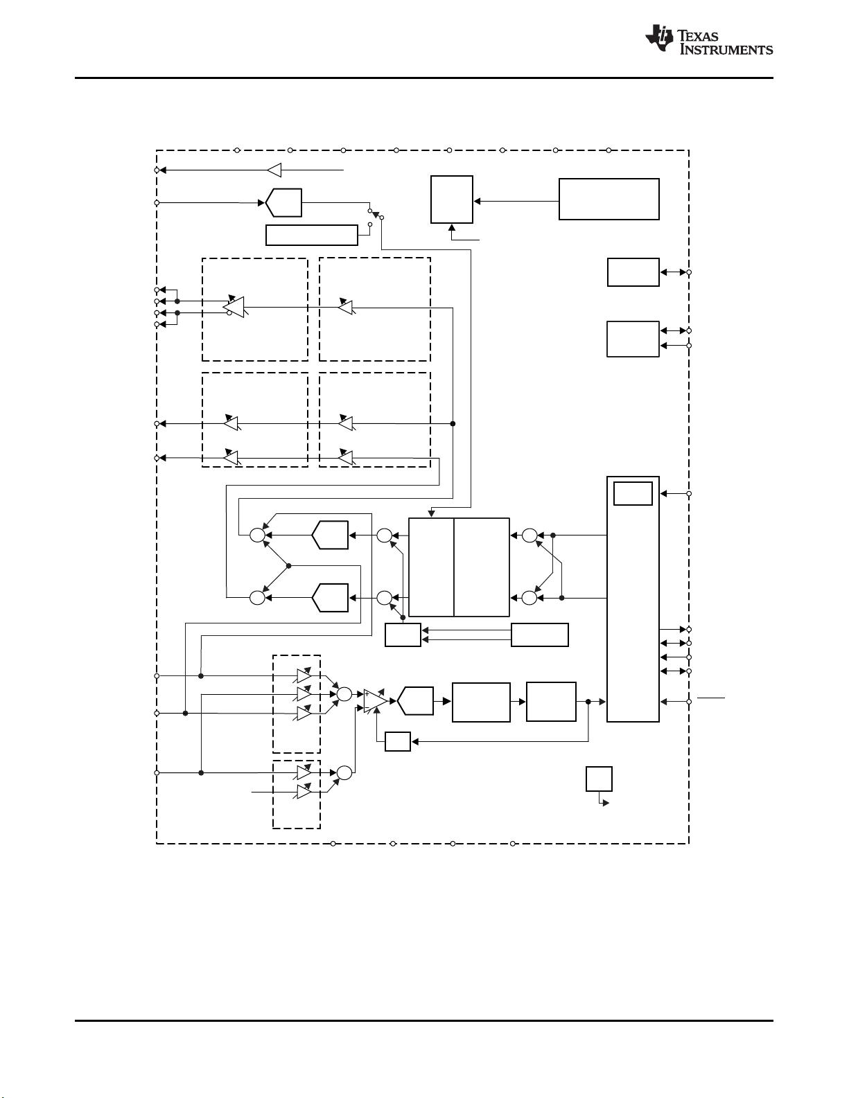
1.3 Description
The TLV320AIC3100 is a low-power, highly integrated, high-performance codec which provides a stereo audio
DAC, a mono audio ADC, and a mono class-D 4-Ω speaker driver.
The TLV320AIC3100 features a high-performance audio codec with 24-bit stereo playback and monaural record
functionality. The device integrates several analog features, such as a microphone interface, headphone drivers,
and speaker drivers. The TLV320AIC3100 has built-in digital audio processing blocks (PRB) for both the DAC
and ADC paths. The digital audio data format is programmable to work with popular audio standard protocols
(I
2
S, left/right-justified) in master, slave, DSP, and TDM modes. Bass boost, treble, or EQ can be supported by
the programmable digital signal-processing block. An on-chip PLL provides the high-speed clock needed by the
digital signal-processing block. The volume level can be controlled by either pin control or by register control. The
audio functions are controlled using the I
2
C serial bus.
The TLV320AIC3100 has a programmable digital sine-wave generator and is available in a 32-pin QFN package.
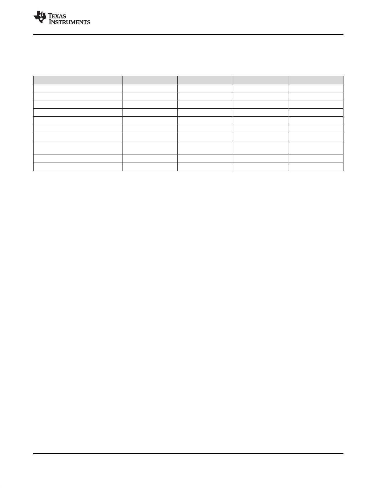
Device Information
(1)
PART NUMBER PACKAGE BODY SIZE (NOM)
TLV320AIC3100 VQFN (32) 5.00 mm × 5.00 mm
(1) For all available packages, see the orderable addendum at the end of the data sheet.
Audio Output Stage
Power Management
RC CLK
Digital
Audio
Processing
and
Serial
Interface
DOUT
DIN
BCLK
WCLK
MCLKPLL
Left and Right Volume-
Control Register
Digital Beep
Generator
Digital
Vol Ctl
Digital Vol
24 dB to
Mute
0 to –63 dB
(1-dB Steps)
DAC
Processing
Blocks
SPKP
SPKP
SPKM
SPKM
Class-D Speaker
Driver
6 dB to 24 dB (6-dB Steps)
Class A/B
Headphone/Lineout
Driver
0 dB to 9 dB (1-dB Steps)
Analog Attenuation
0 dB to –78 dB and Mute
(0.5-dB Steps / Nonlinear)
Analog Attenuation
0 dB to –78 dB and Mute
(0.5-dB Steps / Nonlinear)
HPVDD
SPKVDD SPKVSS
AVDD
AVSSSPKVSSSPKVDD
VOL/
MICDET
HPR
HPL
SCL
SDA
GPIO GPIO1
MIX_L
MIX_R
MIX_L
MIC1LP
DAC_L
MIX_L
DAC_R
MIX_R
RESET
DVDD
DVSS
IOVDD IOVSS
OSC
RC CLK
MIC1LP
Selectable
Gain/Input
Impedance
VCOM
Selectable
Gain/Input
Impedance
P1/R47
0 to 59.5 dB
(0.5-dB steps)
AGC
MIC1RP
I C
2
2 V/2.5 V/AVDD
MICBIAS
Digital Vol
–12..20 dB
Step = 0.5 dB
Mono ADC
Note: Normally,
MCLK is PLL input;
however, BCLK,
GPIO1, etc., can
also be PLL input.
∆-∑
ADC
∆-∑
DAC
∆-
DAC
∑
De-Pop
and
Soft-
Start
P1/R33–R34
P0/R116–R117
P1/R42
P1/R38
P1/R32
P0/R63
P1/R30
P1/R40
P1/R41
P1/R31
P1/R44
P1/R36
P1/R37
P1/R35
P0/R71
P0/R72
P0/R86–R93
P1/R48
P1/R49
Input CM
P1/R50
B0205-08
P0/
R64–R65
P0/R82–R83
HPVSS
MIC1RP
MIC1LM
ADC
Processing
Blocks
7-Bit
Vol
ADC
Σ
Σ
Σ
Σ
Σ
Σ
Σ
Σ
Copyright © 2016, Texas Instruments Incorporated
2
TLV320AIC3100
SLAS667C –NOVEMBER 2009–REVISED OCTOBER 2016
www.ti.com
Submit Documentation Feedback
Product Folder Links: TLV320AIC3100
Device Overview Copyright © 2009–2016, Texas Instruments Incorporated
1.4 Functional Block Diagram
3
TLV320AIC3100
www.ti.com
SLAS667C –NOVEMBER 2009–REVISED OCTOBER 2016
Submit Documentation Feedback
Product Folder Links: TLV320AIC3100
Revision HistoryCopyright © 2009–2016, Texas Instruments Incorporated
Table of Contents
1 Device Overview ......................................... 1
1.1 Features .............................................. 1
1.2 Applications........................................... 1
1.3 Description............................................ 1
1.4 Functional Block Diagram ............................ 2
2 Revision History ......................................... 3
3 Device Comparison ..................................... 5
4 Pin Configuration and Functions..................... 6
4.1 Pin Attributes ......................................... 6
5 Specifications ............................................ 8
5.1 Absolute Maximum Ratings .......................... 8
5.2 ESD Ratings.......................................... 8
5.3 Recommended Operating Conditions ................ 8
5.4 Thermal Information .................................. 9
5.5 Electrical Characteristics ............................. 9
5.6 Power Dissipation Ratings .......................... 11
5.7 I
2
S, LJF, and RJF Timing in Master Mode.......... 11
5.8 I
2
S, LJF, and RJF Timing in Slave Mode ........... 11
5.9 DSP Timing in Master Mode ........................ 11
5.10 DSP Timing in Slave Mode ......................... 12
5.11 I
2
C Interface Timing................................. 12
5.12 Typical Characteristics .............................. 15
6 Parameter Measurement Information .............. 19
7 Detailed Description ................................... 20
7.1 Overview ............................................ 20
7.2 Functional Block Diagram........................... 21
7.3 Feature Description ................................. 21
7.4 Register Map ........................................ 78
8 Application and Implementation................... 120
8.1 Application Information ............................ 120
8.2 Typical Application ................................. 120
9 Power Supply Recommendations................. 123
10 Layout................................................... 124
10.1 Layout Guidelines.................................. 124
10.2 Layout Example.................................... 124
11 Device and Documentation Support.............. 125
11.1 Receiving Notification of Documentation Updates. 125
11.2 Community Resources............................. 125
11.3 Trademarks ........................................ 125
11.4 Electrostatic Discharge Caution ................... 125
11.5 Glossary............................................ 125
12 Mechanical Packaging and Orderable
Information............................................. 125
12.1 Packaging Information ............................. 125
2 Revision History
NOTE: Page numbers for previous revisions may differ from page numbers in the current version.
Changes from Revision B (March 2016) to Revision C Page
• Added Pin 5 (DIN) to the Pin Functions table..................................................................................... 6
Changes from Revision A (May 2012) to Revision B Page
• Added ESD Ratings table, Feature Description section, Device Functional Modes, Application and
Implementation section, Power Supply Recommendations section, Layout section, Device and Documentation
Support section, and Mechanical, Packaging, and Orderable Information section........................................... 1
• Added Power-Supply Sequence section to the Device Initialization section ................................................ 21
• Added the reference to the PGA Gain Versus Input Impedance table in the MICBIAS and Microphone
Preamplifier section ................................................................................................................. 27
• Changed SDIN terminal to DIN in Figure 7-16 .................................................................................. 40
• Changed units from Hz to kHz and updated values to matchTable 7-24.................................................... 41
• Changed Section 7.3.10.1.2 diagrams for PRB_P2/5/8/10/13/15/18/21/24/25 to reflect that the DRC_HPF filter
cannot be bypassed when the DRC is turned off .............................................................................. 43
• Added sequence for inserting a beep in the middle of an already-playing signal and note text following script in
the Key-Click Functionality With Digital Sine-Wave Generator (PRB_P25) section........................................ 58
• Changed less than value or equal to value from 11 MHz to 110 MHz after Equation 11 in PLL section................ 68
• Added note to Register Map section.............................................................................................. 78
• Changed reset values for Page 0 / Register 3 to be more clear.............................................................. 79
• Changed DOSR note in Page 0 / Register 14 by switching multiple value for Filter Type A and Filter Type C........ 81
• Changed description in Page 0 / Register 14 to remove parameters for miniDSP......................................... 81
• Added PRB-modes text the IDAC note in Page 0 / Register 15. Also added Page 0 / Register 15 value note ........ 82
• Added D(3:0) programmed value note to Page 0 / Register 16............................................................... 82
• Changed Page 0 / Register 15 and Page 0 / Register 16 to Reserved...................................................... 82
• Changed Page 0 / Register 20 description ...................................................................................... 83
• Added PRB modes text to note for Page 0 / Register 20...................................................................... 83
4
TLV320AIC3100
SLAS667C –NOVEMBER 2009–REVISED OCTOBER 2016
www.ti.com
Submit Documentation Feedback
Product Folder Links: TLV320AIC3100
Revision History Copyright © 2009–2016, Texas Instruments Incorporated
• Changed Page 0 / Register 21 to Reserved..................................................................................... 83
• Changed Page 0 / Register 22 to Reserved..................................................................................... 83
• Changed Page 0 / Register 66 description from Left-channel to Right-channel ............................................ 94
• Changed values in Page 0 / Register 69 (0x45): DRC Control 2 ............................................................. 95
• Changed Page 0, Register 70, bit D3-D0 decay rate value for 0000 from DR = 1.5625e
–3
to DR = 0.015625 ........ 96
• Switched D1 and D0 descriptions so that D1 is for speaker and D0 is for HP in Page 1 / Register 30 table......... 103
• Changed Page 1 / Register 40, D1 to reserved ............................................................................... 106
• Changed Page 1 / Register 41, D1 to reserved ............................................................................... 106
Changes from Original (November 2009) to Revision A Page
• Added PGA Gain table to Section 7.3.9.1 ....................................................................................... 27
• Deleted Analog Volume Control ... (for D7 = 0) table; modified Analog Volume Control ... (for D7 = 1) table.......... 61
• Added table note to Analog Volume Control table.............................................................................. 61
• Changed page 0 /register 44 to page 1 / register 44 in Section 7.3.10.12.1 ................................................ 62
• Changed max AOSR values in image from 1023, 1024 to 255 and 256. ................................................... 64
• Added missing equations to the PLL section.................................................................................... 68
• Added Timer section................................................................................................................ 69
• Changed bits D1–D0 to Reserved in Page 0 / Register 44.................................................................... 87
• Added table note following Page 0 / Register 64 ............................................................................... 94
• Removed extra character next to LSB in title of Page 0 / Register 75. ...................................................... 97
• Corrected values in Description column of Page 0 / Register 83 ............................................................. 98
• Changed D0 = 1 to Reserved in Page 1 / Register 33 (0x21): HP Output Drivers POP Removal Settings........... 104
• Added table note following Page 1 / Register 40.............................................................................. 106
• Added footnote to Page 1 / Register 41 (0x29): HPR Driver ................................................................ 106
• Deleted table note following Page 1 / Register 48 and Page 1 / Register 49 ............................................. 108
5
TLV320AIC3100
www.ti.com
SLAS667C –NOVEMBER 2009–REVISED OCTOBER 2016
Submit Documentation Feedback
Product Folder Links: TLV320AIC3100
Device ComparisonCopyright © 2009–2016, Texas Instruments Incorporated
3 Device Comparison
Table 3-1. Device Features Comparison
FUNCTION TLV320AIC3100 TLV320AIC3110 TLV320AIC3111 TLV320AIC3120
DACs 2 2 2 1
ADCs 1 1 1 1
Inputs / Outputs 3/3 3/4 3/4 3/2
Resolution (Bits) 16, 20, 24, 32 16, 20, 24, 32 16, 20, 24, 32 16, 20, 24, 32
Control Interface I
2
C I
2
C I
2
C I
2
C
Digital Audio Interface LJ, RJ, I
2
S, TDM, DSP LJ, RJ, I
2
S, TDM, DSP LJ, RJ, I
2
S, TDM, DSP LJ, RJ, I
2
S, TDM, DSP
Number of Digital Audio Interfaces 1 1 1 1
Speaker Amplifier Type Mono Differential
Class-D
Stereo Differential
Class-D
Stereo Differential
Class-D
Mono Differential
Class-D
Configurable miniDSP No No Yes Yes
Headphone Driver Yes Yes Yes Yes
剩余133页未读,继续阅读
安全验证
文档复制为VIP权益,开通VIP直接复制
信息提交成功
评论0
最新资源