TI-LMK04808.pdf
需积分: 5 152 浏览量
2022-11-30
21:49:30
上传
评论 4
收藏 2.11MB PDF 举报

FPGA
DAC
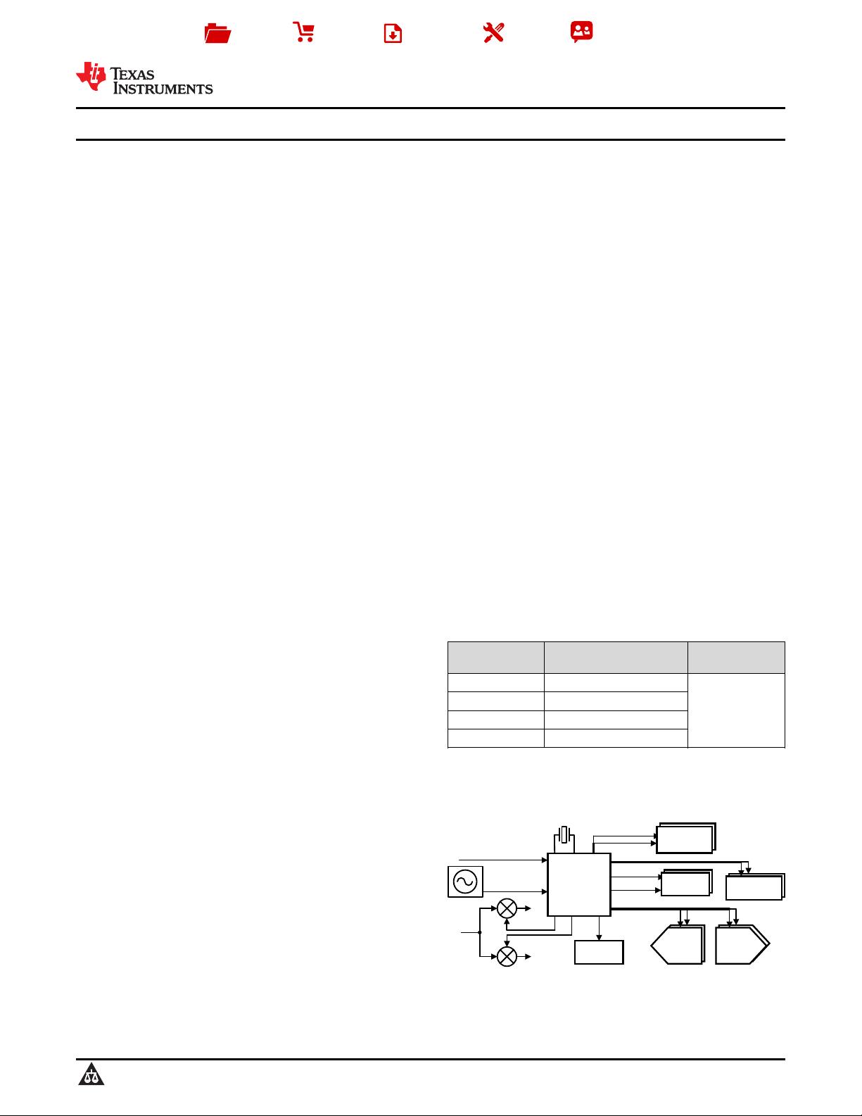
Recovered
³GLUW\´FORFNRU
clean clock
0XOWLSOH³FOHDQ´
clocks at different
frequencies
CLKout4, 5, 6, 7
CLKout2
CLKout0, 1
FPGA
CLKin0
Crystal or
VCXO
Backup
Reference
Clock
CLKin1
OSCout0/
OSCout1
CLKout11
CLKout8A
DAC
CLKout9
IF
I
Q
ADC
LMX2541
PLL+VCO
Serializer/
Deserializer
CPLD
LMK0480x
Precision Clock
Conditioner
CLKout3
Product
Folder
Sample &
Buy
Technical
Documents
Tools &
Software
Support &
Community
LMK04803
,
LMK04805
,
LMK04806
,
LMK04808
SNAS489K –MARCH 2011–REVISED DECEMBER 2014
LMK0480x Low-Noise Clock Jitter Cleaner with Dual Loop PLLs
1 Features 3 Description
The LMK0480x family is the industry's highest
1
• Ultra-Low RMS Jitter Performance
performance clock conditioner with superior clock
– 111 fs RMS Jitter (12 kHz to 20 MHz)
jitter cleaning, generation, and distribution with
– 123 fs RMS Jitter (100 Hz to 20 MHz)
advanced features to meet next generation system
requirements. The dual loop PLLatinum™
• Dual Loop PLLatinum™ PLL Architecture
architecture is capable of 111 fs rms jitter (12 kHz to
• PLL1
20 MHz) using a low noise VCXO module or sub-200
– Integrated Low-Noise Crystal Oscillator Circuit
fs rms jitter (12 kHz to 20 MHz) using a low cost
external crystal and varactor diode.
– Holdover Mode when Input Clocks are Lost
– Automatic or Manual Triggering/Recovery
The dual loop architecture consists of two high-
performance phase-locked loops (PLL), a low-noise
• PLL2
crystal oscillator circuit, and a high-performance
– Normalized PLL Noise Floor of –227 dBc/Hz
voltage controlled oscillator (VCO). The first PLL
– Phase Detector Rate up to 155 MHz
(PLL1) provides low-noise jitter cleaner functionality
while the second PLL (PLL2) performs the clock
– OSCin Frequency-Doubler
generation. PLL1 can be configured to either work
– Integrated Low-Noise VCO
with an external VCXO module or the integrated
• 2 Redundant Input Clocks with LOS
crystal oscillator with an external tunable crystal and
– Automatic and Manual Switch-Over Modes
varactor diode. When paired with a very narrow loop
bandwidth, PLL1 uses the superior close-in phase
• 50 % Duty Cycle Output Divides, 1 to 1045 (Even
noise (offsets below 50 kHz) of the VCXO module or
and Odd)
the tunable crystal to clean the input clock. The
• 12 LVPECL, LVDS, or LVCMOS Programmable
output of PLL1 is used as the clean input reference to
Outputs
PLL2 where it locks the integrated VCO. The loop
bandwidth of PLL2 can be optimized to clean the far-
• Digital Delay: Fixed or Dynamically Adjustable
out phase noise (offsets above 50 kHz) where the
• 25 ps Step Analog Delay Control.
integrated VCO outperforms the VCXO module or
• 14 Differential Outputs. Up to 26 Single Ended.
tunable crystal used in PLL1.
– Up to 6 VCXO/Crystal Buffered Outputs
Device Information
• Clock Rates of up to 1536 MHz
REFERENCE
• 0-Delay Mode
PART NUMBER VCO FREQUENCY
INPUTS
• Three Default Clock Outputs at Power Up
LMK04803 1840 to 2030 MHz
• Multi-Mode: Dual PLL, Single PLL, and Clock
LMK04805 2148 to 2370 MHz
2
Distribution
LMK04806 2370 to 2600 MHz
• Industrial Temperature Range: –40 to 85°C
LMK04808 2750 to 3072 MHz
• 3.15-V to 3.45-V Operation
(1) For all available packages, see the orderable addendum at
the end of the datasheet.
• 2 Dedicated Buffered/Divided OSCin Clocks
• Package: 64-Pin WQFN (9.0 × 9.0 × 0.8 mm)
Simplified Schematic
2 Applications
• Data Converter Clocking
• Wireless Infrastructure
• Networking, SONET/SDH, DSLAM
• Medical / Video / Military / Aerospace
• Test and Measurement
1
An IMPORTANT NOTICE at the end of this data sheet addresses availability, warranty, changes, use in safety-critical applications,
intellectual property matters and other important disclaimers. PRODUCTION DATA.


剩余138页未读,继续阅读
资源评论


不觉明了
- 粉丝: 3230
- 资源: 5614


最新资源
- 藏区特产销售平台源代码+论文+毕业设计.zip
- B297C8EC5A69641DB3E681E1B3F894E5.mp4
- PrimitivesPro v2.2.unitypackage
- 财务管理系统源代码+论文.zip
- 高级信息通信运行管理员第七套试卷
- UModeler v2.11.6 (May 10, 2024).unitypackage
- 基于Selenium的Java爬虫实战(内含谷歌浏览器Chrom和Chromedriver版本127.0.6486.0)
- 基于FPGA的CORDIC算法旋转模式实现
- bilibili视频解析下载源码
- 基于Selenium的Java爬虫实战(内含谷歌浏览器Chrom和Chromedriver版本124.0.6367.60)
资源上传下载、课程学习等过程中有任何疑问或建议,欢迎提出宝贵意见哦~我们会及时处理!
点击此处反馈


