没有合适的资源?快使用搜索试试~ 我知道了~
TI-THS1041.pdf
需积分: 5 0 下载量 55 浏览量
2022-11-27
16:20:39
上传
评论 4
收藏 1.17MB PDF 举报
温馨提示
试读
42页
TI-THS1041.pdf
资源详情
资源评论
SLAS289C − OCTOBER 2001 − REVISED OCTOBER 2004
1
www.ti.com
FEATURES
D
Analog Supply 3 V
D Digital Supply 3 V
D Configurable Input Functions:
− Single-Ended
− Single-Ended With Analog Clamp
− Single-Ended With Programmable Digital
Clamp
− Differential
D Built-In Programmable Gain Amplifier (PGA)
D Differential Nonlinearity: ±0.45 LSB
D Signal-to-Noise: 60 dB Typ f
(IN)
at 4.8 MHz
D Spurious Free Dynamic Range: 72 dB
D Adjustable Internal Voltage Reference
D Unsigned Binary/2s Complement Output
D Out-of-Range Indicator
D Power-Down Mode
APPLICATIONS
D
Video/CCD Imaging
D Communications
D Set-Top-Box
D Medical
DESCRIPTION
The THS1041 is a CMOS, low power, 10-bit, 40 MSPS
analog-to-digital converter (ADC) that operates from a
single 3-V supply. The THS1041 has been designed to
give circuit developers flexibility. The analog input to the
THS1041 can be either single-ended or differential.
This device has a built-in clamp amplifier whose clamp
input level can be driven from an external dc source or
from an internal high-precision 10-bit digital clamp level
programmable via an internal CLAMP register. A 3-bit
PGA is included to maintain SNR for small signals. The
THS1041 provides a wide selection of voltage
references to match the user’s design requirements.
For more design flexibility, the internal reference can be
bypassed to use an external reference to suit the dc
accuracy and temperature drift requirements of the
application. The out-of-range output indicates any
out-of-range condition in THS1041’s input signal. The
format of the digital output can be coded in either
unsigned binary or 2s complement.
The speed, resolution, and single-supply operation of
the THS1041 are suited to applications in set-top-box
(STB), video, multimedia, imaging, high-speed
acquisition, and communications. The built-in clamp
function allows dc restoration of a video signal and is
suitable for video applications. The speed and
resolution ideally suit charge-couple device (CCD) input
systems such as color scanners, digital copiers, digital
cameras, and camcorders. A wide input voltage range
allows the THS1041 to be applied in both imaging and
communications systems.
The THS1041C is characterized for operation from 0°C
to 70°C, while the THS1041I is characterized for
operation from −40°C to 85°C.
! " #$% !" &$'(#! )!%*
)$#" # "&%##!" &% +% %" %,!" "$%"
"!)!) -!!.* )$# &#%""/ )%" %#%""!(. #($)%
%"/ !(( &!!%%"*
Copyright 2002 − 2004, Texas Instruments Incorporated
Please be aware that an important notice concerning availability, standard warranty, and use in critical applications of
Texas Instruments semiconductor products and disclaimers thereto appears at the end of this data sheet.
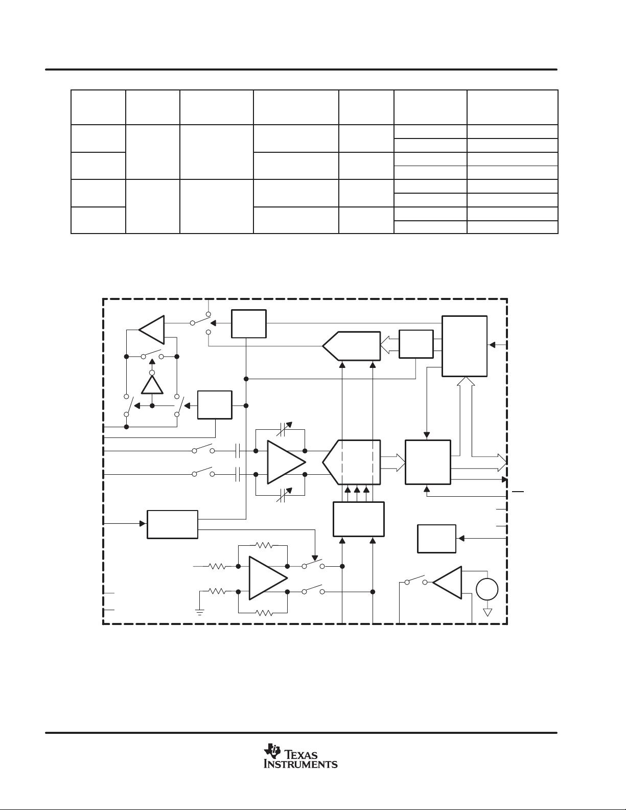
1
2
3
4
5
6
7
8
9
10
11
12
13
14
28
27
26
25
24
23
22
21
20
19
18
17
16
15
AGND
DV
DD
I/O0
I/O1
I/O2
I/O3
I/O4
I/O5
I/O6
I/O7
I/O8
I/O9
OVR
DGND
AV
DD
AIN+
VREF
AIN−
REFB
MODE
REFT
CLAMPOUT
CLAMPIN
CLAMP
REFSENSE
WR
OE
CLK
28-PIN TSSOP/SOIC PACKAGE
(TOP VIEW)
SLAS289C − OCTOBER 2001 − REVISED OCTOBER 2004
2
www.ti.com
AVAILABLE OPTIONS
PRODUCT
PACKAGE
LEAD
PACKAGE
DESGIGNATOR
†
SPECIFIED
TEMPERATURE
RANGE
PACKAGE
MARKINGS
ORDERING
NUMBER
TRANSPORT MEDIA,
QUANTITY
THS1041C
0°C to 70°C
TH1041
THS1041CPW Tube, 50
THS1041C
TSSOP−28
PW
0°C to 70°C TH1041
THS1041CPWR Tube and Reel, 2000
THS1041I
TSSOP−28 PW
−40°C to 85°C
TJ1041
THS1041IPW Tube, 50
THS1041I −40°C to 85°C TJ1041
THS1041IPWR Tube and Reel, 2000
THS1041C
0°C to 70°C
TH1041
THS1041CDW Tube, 20
THS1041C
SOP−28
DW
0°C to 70°C TH1041
THS1041CDWR Tube and Reel, 1000
THS1041I
SOP−28 DW
−40°C to 85°C
TJ1041
THS1041IDW Tube, 20
THS1041I −40°C to 85°C TJ1041
THS1041IDWR Tube and Reel, 1000
†
For the most current specification and package information, refer to the TI web site at www.ti.com.
functional block diagram
10 Bit
DAC
SHPGA
10 Bit
ADC
ADC
Reference
Resistor
Digital
Interface
3-State
Output
Buffers
Mode
Detection
0.5 V
CLAMPOUT
CLAMP
AIN+
AIN−
MODE
REFSENSE
VREF
REFB REFT
WR
I/O (0−9)
OVR
OE
Timing
Circuit
CLK
AV
DD
AGND
CLAMPIN
Clamp
Logic
Clamp
Logic
Clamp
Logic
A2
+
−
A1
VREF
DV
DD
DGND
NOTE: A1 − Internal bandgap reference
A2 − Internal ADC reference generator
SLAS289C − OCTOBER 2001 − REVISED OCTOBER 2004
3
www.ti.com
Terminal Functions
TERMINAL
I/O
DESCRIPTION
NAME NO.
I/O
DESCRIPTION
AGND 1 I Analog ground
AIN+ 27 I Positive analog input
AIN− 25 I Negative analog input
AV
DD
28 I Analog supply
CLAMP 19 I High to enable clamp mode, low to disable clamp mode
CLAMPIN 20 I Connect to an external analog clamp reference input.
CLAMPOUT 21 O
The CLAMPOUT pin can provide a dc restoration or a bias source function (see AC reference generation
section). If neither function is required then the clamp can be disabled to save power (see power management
section).
CLK 15 I Clock input
DGND 14 I Digital ground
DV
DD
2 I Digital supply
I/O0
I/O1
I/O2
I/O3
I/O4
I/O5
I/O6
I/O7
I/O8
I/O9
3
4
5
6
7
8
9
10
11
12
I/O
Digital I/O bit 0 (LSB)
Digital I/O bit 1
Digital I/O bit 2
Digital I/O bit 3
Digital I/O bit 4
Digital I/O bit 5
Digital I/O bit 6
Digital I/O bit 7
Digital I/O bit 8
Digital I/O bit 9 (MSB)
MODE 23 I Operating mode select (AGND, AV
DD
/2, AV
DD
)
OE 16 I High to high-impedance state the data bus, low to enable the data bus
OVR 13 O Out-of-range indicator
REFB 24 I/O Bottom ADC reference voltage
REFSENSE 18 I VREF mode control
REFT 22 I/O Top ADC reference voltage
VREF 26 I/O Internal or external reference
WR 17 I Write strobe
SLAS289C − OCTOBER 2001 − REVISED OCTOBER 2004
4
www.ti.com
absolute maximum ratings over operating free-air temperature (unless otherwise noted)
†
Supply voltage range: AV
DD
to AGND, DV
DD
to DGND −0.3 V to 4 V. . . . . . . . . . . . . . . . . . . . . . . . . . . . . . . . . . . . . .
AGND to DGND −0.3 V to 0.3 V. . . . . . . . . . . . . . . . . . . . . . . . . . . . . . . . . . . . . . . . . . . . . . . . . . .
AV
DD
to DV
DD
−4 V to 4 V. . . . . . . . . . . . . . . . . . . . . . . . . . . . . . . . . . . . . . . . . . . . . . . . . . . . . . .
MODE input voltage range, MODE to AGND −0.3 V to AV
DD
+ 0.3 V. . . . . . . . . . . . . . . . . . . . . . . . . . . . . . . . . . . . . . .
Reference voltage input range, REFT, REFB, to AGND −0.3 V to AV
DD
+ 0.3 V. . . . . . . . . . . . . . . . . . . . . . . . . . . . .
Analog input voltage range, AIN to AGND −0.3 V to AV
DD
+ 0.3 V. . . . . . . . . . . . . . . . . . . . . . . . . . . . . . . . . . . . . . . . .
Reference input voltage range, VREF to AGND −0.3 V to AV
DD
+ 0.3 V. . . . . . . . . . . . . . . . . . . . . . . . . . . . . . . . . . . .
Reference output voltage range, VREF to AGND −0.3 V to AV
DD
+ 0.3 V. . . . . . . . . . . . . . . . . . . . . . . . . . . . . . . . . . .
Clock input voltage range, CLK to AGND −0.3 V to AV
DD
+ 0.3 V. . . . . . . . . . . . . . . . . . . . . . . . . . . . . . . . . . . . . . . . . .
Digital input voltage range, digital input to DGND −0.3 V to DV
DD
+ 0.3 V. . . . . . . . . . . . . . . . . . . . . . . . . . . . . . . . . . .
Digital output voltage range, digital output to DGND −0.3 V to DV
DD
+ 0.3 V. . . . . . . . . . . . . . . . . . . . . . . . . . . . . . . .
Operating junction temperature range, T
J
0°C to 150°C. . . . . . . . . . . . . . . . . . . . . . . . . . . . . . . . . . . . . . . . . . . . . . . . . .
Storage temperature range, T
stg
−65°C to 150°C. . . . . . . . . . . . . . . . . . . . . . . . . . . . . . . . . . . . . . . . . . . . . . . . . . . . . . .
Lead temperature 1,6 mm (1/16 in) from case for 10 seconds 300°C. . . . . . . . . . . . . . . . . . . . . . . . . . . . . . . . . . . . . . .
†
Stresses beyond those listed under “absolute maximum ratings” may cause permanent damage to the device. These are stress ratings only, and
functional operation of the device at these or any other conditions beyond those indicated under “recommended operating conditions” is not
implied. Exposure to absolute-maximum-rated conditions for extended periods may affect device reliability.
recommended operating conditions
over operating free-air temperature range T
A
, (unless otherwise noted)
PARAMETER CONDITION MIN NOM MAX UNIT
Power Supply
Supply voltage AV
DD
, DV
DD
3 3 3.6 V
Analog and Reference Inputs
VREF input voltage V
I(VREF)
REFSENSE = AV
DD
0.5 1 V
REFT input voltage V
I(REFT)
MODE = AGND 1.75 2 V
REFB input voltage V
I(REFB)
MODE = AGND 1 1.25 V
Reference input voltage V
I(REFT)
−
V
I(REFB)
MODE = AGND 0.5 1 V
Reference common mode voltage (V
I(REFT)
+
V
I(REFB)
)/2 MODE = AGND (AV
DD
/2) − 0.05 (AV
DD
/2) + 0.05 V
Analog input voltage differential (see Note 1)
V
I(AIN)
REFSENSE = AGND −1 1 V
Analog input voltage differential (see Note 1) V
I(AIN)
REFSENSE = VREF −0.5 0.5 V
Analog input capacitance, C
I
10 pF
Clock input (see Note 2) 0 AV
DD
V
Clamp input voltage V
I(CLAMPIN)
0.1 AV
DD
− 0.1 V
Digital Outputs
Maximum digital output load resistance R
L
100 kΩ
Maximum digital output load capacitance C
L
10 pF
Digital Inputs
High-level input voltage, V
IH
2.4 DV
DD
V
Low-level input voltage, V
IL
DGND 0.8 V
Clock frequency (see Note 3) t
c
f
(CLK)
= 5 MHz to 40 MHz 25 200 nS
Clock pulse duration t
w(CKL),
t
w(CKH)
f
(CLK)
= 40 MHz 11.25 12.5 13.75 nS
Operating free-air temperature, T
A
THS1041C 0 70
°C
Operating free-air temperature, T
A
THS1041I −40 85
°
C
NOTE 1: V
I(AIN)
is AIN+ − AIN− range, based on V
I(REFT)
−
V
I(REFB)
= 1 V. Varies proportional to the V
I(REFT)
−
V
I(REFB)
value. Input common mode
voltage is recommended to be AV
DD
/2.
NOTE 2: The clock pin is referenced to AV
SS
and powered by AV
DD
.
NOTE 3: Clock frequency can be extended to this range without degradation of performance.
SLAS289C − OCTOBER 2001 − REVISED OCTOBER 2004
5
www.ti.com
electrical characteristics
over recommended operating conditions, AV
DD
= 3 V, DV
DD
= 3 V, f
s
= 40 MSPS/50% duty cycle, MODE = AV
DD
(internal reference),
differential input range = 1 Vpp and 2 Vpp, PGA = 1X, T
A
= T
min
to T
max
(unless otherwise noted)
power supply
PARAMETER TEST CONDITIONS MIN TYP MAX UNIT
AV
DD
Supply voltage
3 3 3.6
V
DV
DD
Supply voltage
3 3 3.6
V
I
CC
Operating supply current See Note 4 34 42 mA
P
D
Power dissipation See Note 4 103 125 mW
P
D(STBY)
Standby power 75 µW
Power up time for all references from standby, t
(PU)
10 µF bypass 770 µs
Wake-up time, t
(WU)
See Note 5 45 µs
REFT, REFB internal ADC reference voltages outputs (MODE = AV
DD
or AV
DD
/2) (See Note 6)
PARAMETER TEST CONDITIONS MIN TYP MAX UNIT
Reference voltage top, REFT
VREF = 0.5 V
AV
DD
= 3 V
1.75
V
Reference voltage top, REFT
VREF = 1 V
AV
DD
= 3 V
2
V
Refence voltage bottom, REFB
VREF = 0.5 V
AV
DD
= 3 V
1.25
V
Refence voltage bottom, REFB
VREF = 1 V
AV
DD
= 3 V
1
V
Input resistance between REFT and REFB 1.4 1.9 2.5 kΩ
VREF (on-chip voltage reference generator)
PARAMETER MIN TYP MAX UNIT
Internal 0.5-V reference voltage (REFSENSE = VREF) 0.45 0.5 0.55 V
Internal 1-V reference voltage (REFSENSE = AGND) 0.95 1 1.05 V
Reference input resistance (REFSENSE = AV
DD
, MODE = AV
DD
/2 or AV
DD
) 7 14 21 kΩ
dc accuracy
PARAMETER MIN TYP MAX UNIT
Resolution 10 Bits
INL Integral nonlinearity (see definitions) −1.5 ± 0.75 1.5 LSB
DNL Differential nonlinearity (see definitions) −0.9 ±0.3 1 LSB
Zero error (see definitions) −1.5 0.7 1.5 %FSR
Full-scale error (see definitions) −3 2.2 3 %FSR
Missing code No missing code assured
NOTES: 4. A −1 dBFS 10-KHz triangle wave is applied at AIN+ and AIN−. Internal bandgap reference and ADC reference are enabled,
CLAMPOUT is set to AV
DD
/2. ADC conversions are taking place during power measurements at 40 MSPS. A CLAMPOUT load or
VREF load may result in additional current.
5. Wake-up time is from the power-down state to accurate ADC samples being taken and is specified for MODE = AGND with external
reference sources applied to the device at the time of release of power-down and an applied 40-MHz clock. Circuits that need to
power up are the bandgap, bias generator, ADC, and SHPGA.
6. External reference values are listed in the Recommended Operating Conditions Table.
剩余41页未读,继续阅读
安全验证
文档复制为VIP权益,开通VIP直接复制
信息提交成功
评论0
最新资源