没有合适的资源?快使用搜索试试~ 我知道了~
TI-REF4132-Q1.pdf
需积分: 5 0 下载量 141 浏览量
2022-11-20
16:34:27
上传
评论 5
收藏 1.87MB PDF 举报
温馨提示
![preview](https://dl-preview.csdnimg.cn/87096622/0001-e1e51bbdc2c85010c26322a05339f373_thumbnail.jpeg)
![preview-icon](https://csdnimg.cn/release/downloadcmsfe/public/img/scale.ab9e0183.png)
试读
26页
TI-REF4132-Q1.pdf
资源推荐
资源详情
资源评论
![](https://csdnimg.cn/release/download_crawler_static/87096622/bg1.jpg)
REF4132-Q1
+
±
OPA735
+5 V
+5 V
-5 V
-2.5 V
+2.5 V
EN VIN
VREF
GND
N/C
R
1
10 NŸ
R
2
10 NŸ
Load Current (mA)
Dropout Voltage (V)
0
0.04
0.08
0.12
0.16
0.2
0.24
0.28
0.32
0.36
0.4
5 100
+25°C
-40°C
+125°C
D001
Product
Folder
Order
Now
Technical
Documents
Tools &
Software
Support &
Community
Reference
Design
An IMPORTANT NOTICE at the end of this data sheet addresses availability, warranty, changes, use in safety-critical applications,
intellectual property matters and other important disclaimers. PRODUCTION DATA.
REF4132-Q1
SNAS795A –FEBRUARY 2020–REVISED JULY 2020
REF4132-Q1 Low-Drift, Low-Power, Small-Footprint Series Voltage Reference
1
1 Features
1
• Qualified for automotive applications
• AEC-Q100 qualified with the following results:
– Device temperature grade 1: –40ºC to +125ºC
ambient operating temperature range
– Device HBM ESD classification level 2
• Voltage options: 2.5V, 3V, 3.3V, 4.096V, 5V
• Initial accuracy: ±0.05% (maximum)
• Temperature coefficient : A grade: 12 ppm/°C
(maximum) B grade: 30 ppm/°C (maximum)
• Operating temperature range: −40°C to +125°C
• Output current: ±10 mA
• Low quiescent current: 100 μA (maximum)
• Output 1/f noise (0.1 Hz to 10 Hz): 15 µV
PP
/V
• Excellent long-term stability 30 ppm/1000 hrs
• Small footprint 5-pin SOT-23 package
2 Applications
• ADAS front camera
• ADAS surround view system ECU
• Traction inverter
• Automotive DC/DC converter
• HEV/EV On-board (OBC) & wireless charger
3 Description
The REF4132-Q1 device is a low temperature drift
(12 ppm/°C), low-power, high-precision CMOS
voltage reference, featuring ± 0.05% initial accuracy,
low operating current with power consumption less
than 100μA. This device also offers very low output
noise of 15 μV
p-p
/V, which enables its ability to
maintain high signal integrity with high-resolution data
converters in noise critical systems. Packaged in the
same SOT-23-5 package, REF4132-Q1 offers
enhanced specifications and pin-to-pin replacement
for LM4128-Q1 and LM4132-Q1.
Stability and system reliability are further improved by
the low output-voltage hysteresis of the device and
low long-term output voltage drift. Furthermore, the
small size and low operating current of the devices
(100 μA) can benefit portable and battery-powered
applications.
REF4132-Q1 is specified for the wide temperature
range of −40°C to +125°C.
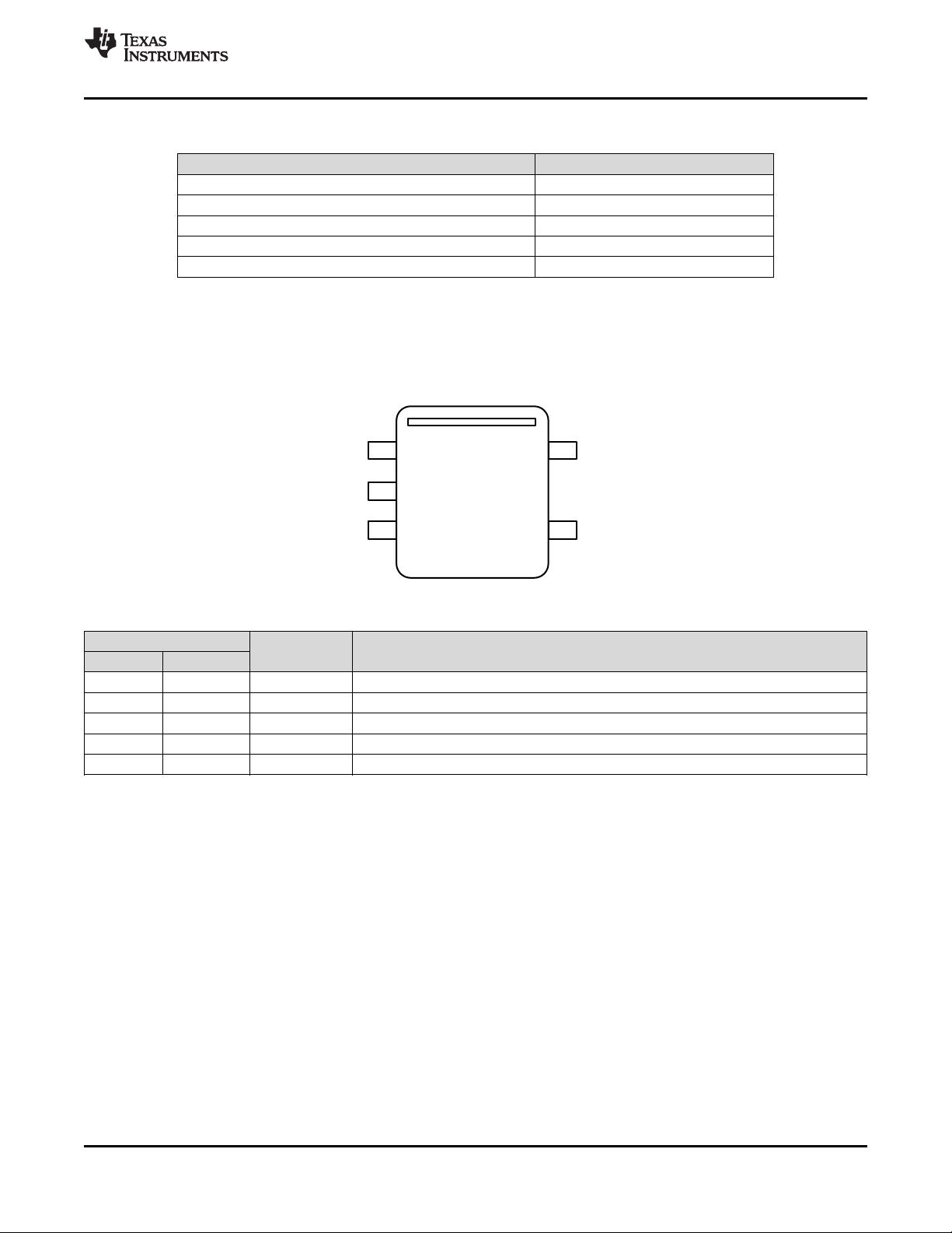
Device Information
(1)
PART NAME PACKAGE BODY SIZE (NOM)
REF4132-Q1 SOT-23 (5) 2.90 mm × 1.60 mm
(1) For all available packages, see the orderable addendum at
the end of the data sheet.
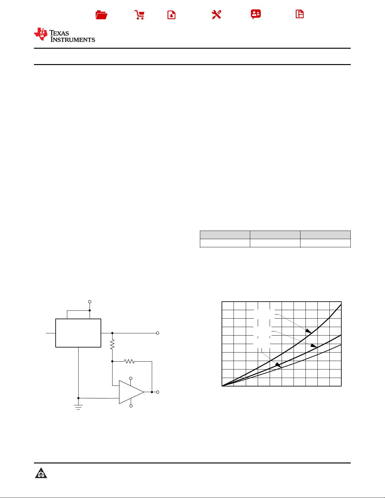
Simplified Schematic Dropout vs. Current Load Over Temperature
![](https://csdnimg.cn/release/download_crawler_static/87096622/bg2.jpg)
2
REF4132-Q1
SNAS795A –FEBRUARY 2020–REVISED JULY 2020
www.ti.com
Product Folder Links: REF4132-Q1
Submit Documentation Feedback Copyright © 2020, Texas Instruments Incorporated
Table of Contents
1 Features.................................................................. 1
2 Applications ........................................................... 1
3 Description ............................................................. 1
4 Revision History..................................................... 2
5 Device Comparison Table..................................... 3
6 Pin Configuration and Functions......................... 3
7 Specifications......................................................... 4
7.1 Absolute Maximum Ratings ...................................... 4
7.2 ESD Ratings.............................................................. 4
7.3 Recommended Operating Conditions....................... 4
7.4 Thermal Information.................................................. 4
7.5 Electrical Characteristics........................................... 5
7.6 Typical Characteristics.............................................. 6
8 Parameter Measurement Information ................ 10
8.1 Solder Heat Shift..................................................... 10
8.2 Long-Term Stability................................................. 11
8.3 Thermal Hysteresis ................................................. 11
8.4 Power Dissipation ................................................... 12
8.5 Noise Performance ................................................. 12
9 Detailed Description ............................................ 13
9.1 Overview ................................................................. 13
9.2 Functional Block Diagram ....................................... 13
9.3 Feature Description................................................. 13
9.4 Device Functional Modes........................................ 14
10 Application and Implementation........................ 15
10.1 Application Information.......................................... 15
10.2 Typical Application: Basic Voltage Reference
Connection............................................................... 15
11 Power Supply Recommendations ..................... 17
12 Layout................................................................... 17
12.1 Layout Guidelines ................................................. 17
12.2 Layout Example .................................................... 17
13 Device and Documentation Support ................. 18
13.1 Documentation Support ........................................ 18
13.2 Receiving Notification of Documentation Updates 18
13.3 Support Resources ............................................... 18
13.4 Trademarks........................................................... 18
13.5 Electrostatic Discharge Caution............................ 18
13.6 Glossary................................................................ 18
14 Mechanical, Packaging, and Orderable
Information ........................................................... 18
4 Revision History
NOTE: Page numbers for previous revisions may differ from page numbers in the current version.
Changes from Original (February 2020) to Revision A Page
• APL to RTM release. .............................................................................................................................................................. 1
![](https://csdnimg.cn/release/download_crawler_static/87096622/bg3.jpg)
1 5
2
3 4
Not to scale
N/C
GND
EN
VREF
VIN
3
REF4132-Q1
www.ti.com
SNAS795A –FEBRUARY 2020–REVISED JULY 2020
Product Folder Links: REF4132-Q1
Submit Documentation FeedbackCopyright © 2020, Texas Instruments Incorporated
5 Device Comparison Table
PRODUCT V
OUT
REF4132 - 2.5 2.5 V
REF4132 - 3.0 3 V
REF4132 - 3.3 3.3 V
REF4132 - 4.0 4.096 V
REF4132 - 5.0 5 V
6 Pin Configuration and Functions
DBV Package
5-Pin SOT-23
Top View
Pin Functions
PIN
TYPE DESCRIPTION
NO. NAME
1 N/C – No connect pin, leave floating
2 GND Ground Ground
3 EN I/O Enable pin. Enables or disables the device.
4 VIN Power Input supply
5 VREF Output Reference output
![](https://csdnimg.cn/release/download_crawler_static/87096622/bg4.jpg)
4
REF4132-Q1
SNAS795A –FEBRUARY 2020–REVISED JULY 2020
www.ti.com
Product Folder Links: REF4132-Q1
Submit Documentation Feedback Copyright © 2020, Texas Instruments Incorporated
(1) Stresses above these ratings may cause permanent damage. Exposure to absolute maximum conditions for extended periods may
degrade device reliability. These are stress ratings only, and functional operation of the device at these or any other conditions beyond
those specified is not implied. These are stress ratings only and functional operation of the device at these or any other conditions
beyond those specified in the Electrical Characteristics Table is not implied.
7 Specifications
7.1 Absolute Maximum Ratings
over operating free-air temperature range (unless otherwise noted)
(1)
MIN MAX UNIT
Input voltage V
IN
–0.3 6 V
Enable voltage V
EN
–0.3 V
IN
+ 0.3 V
Output voltage V
REF
–0.3 5.5 V
Output short circuit current I
SC
20 mA
Operating temperature range T
A
–55 150 °C
Storage temperature range Tstg –65 170 °C
(1) AEC Q100-002 indicates that HBM stressing shall be in accordance with the ANSI/ESDA/JEDEC JS-001 specification.
7.2 ESD Ratings
VALUE UNIT
V
(ESD)
Electrostatic discharge
Human-body model (HBM), per AEC Q100-
002
(1)
±2500
V
Charged-device model (CDM), per AEC Q100-
011
±1500
(1) Dropout voltage
7.3 Recommended Operating Conditions
over operating free-air temperature range (unless otherwise noted)
MIN NOM MAX UNIT
V
IN
Input Voltage
V
REF
+
V
DO
(1)
5.5 V
V
EN
Enable Voltage 0 V
IN
V
I
L
Output Current –10 10 mA
T
A
Operating Temperature –40 25 125 ℃
(1) For more information about traditional and new thermal metrics, see the Semiconductor and IC Package Thermal Metrics application
report.
7.4 Thermal Information
THERMAL METRIC
(1)
DEVICE
UNITDBV
5 PINS
R
θJA
Junction-to-ambient thermal resistance 185 °C/W
R
θJC(top)
Junction-to-case (top) thermal resistance 156 °C/W
R
θJB
Junction-to-board thermal resistance 29.6 °C/W
Ψ
JT
Junction-to-top characterization parameter 33.8 °C/W
Ψ
JB
Junction-to-board characterization parameter 29.1 °C/W
R
θJC(bot)
Junction-to-case (bottom) thermal resistance N/A °C/W
![](https://csdnimg.cn/release/download_crawler_static/87096622/bg5.jpg)
5
REF4132-Q1
www.ti.com
SNAS795A –FEBRUARY 2020–REVISED JULY 2020
Product Folder Links: REF4132-Q1
Submit Documentation FeedbackCopyright © 2020, Texas Instruments Incorporated
(1) At higher ambient temperature the short circuit current capacity is limited due to junction temeprature max limit
7.5 Electrical Characteristics
At V
IN
= 5.5 V, V
EN
= V
IN
, C
REF
= 10 µF, C
IN
= 0.1 µF, I
L
= 0 mA, minimum and maximum specifications at T
A
= –40℃ to
125℃; typical specifications at T
A
= 25℃ unless otherwise noted
PARAMETER TEST CONDITION MIN TYP MAX UNIT
ACCURACY AND DRIFT
Output voltage
accuracy
T
A
= 25°C –0.05 0.05 %
Output voltage
temperature
coefficient
–40°C ≤ T
A
≤ 125°C REF4132 A grade 12 ppm/℃
–40°C ≤ T
A
≤ 125°C REF4132 B grade 30 ppm/℃
LINE & LOAD REGULATION
ΔV
REF
/ΔV
IN
Line Regulation
V
REF
+ V
DO
≤ V
IN
≤ 5.5 V 2 ppm/V
V
REF
+ V
DO
≤ V
IN
≤ 5.5 V 15 ppm/V
V
REF
= 5 V, V
REF
+ V
DO
≤ V
IN
≤ 5.5 V 55 ppm/V
ΔV
REF
/ΔI
L
Load Regulation
I
L
= 0 mA to 10mA, V
IN
= V
REF
+ V
DO
20 ppm/mA
I
L
= 0 mA to 10mA, V
IN
= V
REF
+ V
DO
120 ppm/mA
POWER SUPPLY
V
IN
Input voltage
V
REF
+
V
DO
5.5 V
I
Q
Quiescent current
Active mode 80 100 µA
Shutdown mode, V
EN
= 0 V 2.5 5 µA
V
EN
Enable pin
Voltage
Voltage reference in active mode (EN=1) 1.6 V
Voltage reference in shutdown mode (EN=0) 0.5 V
I
EN
Enable pin
current
V
EN
= 5.5 V 1 2 µA
V
DO
Dropout voltage
I
L
= 0 mA 50 mV
I
L
= 0 mA 100 mV
I
L
= 10 mA 500 mV
I
SC
Short circuit current
(1)
V
REF
= 0 V 18 11.5 mA
TURNON
t
ON
Turn-on time 0.1% settling, C
L
= 1 µF, 10% to 90% 2.5 ms
NOISE
e
n(p-p)
Low frequency
noise
ƒ = 0.1 Hz to 10 Hz 15 ppm
p-p
e
n
Wide band
noise
ƒ = 10 Hz to 10 kHz 24 µV
rms
HYSTERESIS AND LONG-TERM STABILITY
Long-term stability 0 to 1000h at 35℃ 30 ppm
V
HYST
Output voltage
hysteresis
T
A
= 25℃ to −40℃ to 125℃ to 25℃ 35 ppm
CAPACITIVE LOAD
C
L
Stable output
capacitor range
0.1 10 µF
剩余25页未读,继续阅读
资源评论
![avatar-default](https://csdnimg.cn/release/downloadcmsfe/public/img/lazyLogo2.1882d7f4.png)
![avatar](https://profile-avatar.csdnimg.cn/107303f5121d47e49d12d0a9ae68af10_weixin_54787054.jpg!1)
不觉明了
- 粉丝: 3231
- 资源: 5614
上传资源 快速赚钱
我的内容管理 展开
我的资源 快来上传第一个资源
我的收益
登录查看自己的收益我的积分 登录查看自己的积分
我的C币 登录后查看C币余额
我的收藏
我的下载
下载帮助
![voice](https://csdnimg.cn/release/downloadcmsfe/public/img/voice.245cc511.png)
![center-task](https://csdnimg.cn/release/downloadcmsfe/public/img/center-task.c2eda91a.png)
安全验证
文档复制为VIP权益,开通VIP直接复制
![dialog-icon](https://csdnimg.cn/release/downloadcmsfe/public/img/green-success.6a4acb44.png)