没有合适的资源?快使用搜索试试~ 我知道了~
TI-TPS2010A.pdf
需积分: 9 0 下载量 39 浏览量
2022-11-14
22:28:55
上传
评论 5
收藏 1.45MB PDF 举报
温馨提示
试读
30页
TI-TPS2010A.pdf
资源推荐
资源详情
资源评论
1
FEATURES
DESCRIPTION
TPS2014600mA
TPS20151 A
TPS2041B500mA
TPS2051B500mA
TPS2045A 250mA
TPS2049100mA
TPS2055A 250mA
TPS20611 A
TPS20651 A
TPS20681.5 A
TPS20691.5 A
TPS201xA 0.2 A -2 A
TPS202x0.2 A -2 A
TPS203x0.2 A -2 A
TPS2010A, TPS2011A
TPS2012A, TPS2013A
SLVS189C – DECEMBER 1998 – REVISED SEPTEMBER 2007
www.ti.com
POWER-DISTRIBUTION SWITCHES
• 33-m Ω (5-V Input) High-Side MOSFET Switch
• Short-Circuit and Thermal Protection
• Operating Range . . . 2.7 V to 5.5 V
• Logic-Level Enable Input
• Typical Rise Time. . . 6.1 ms
• Undervoltage Lockout
• Maximum Standby Supply Current. . . 10 μ A
• No Drain-Source Back-Gate Diode
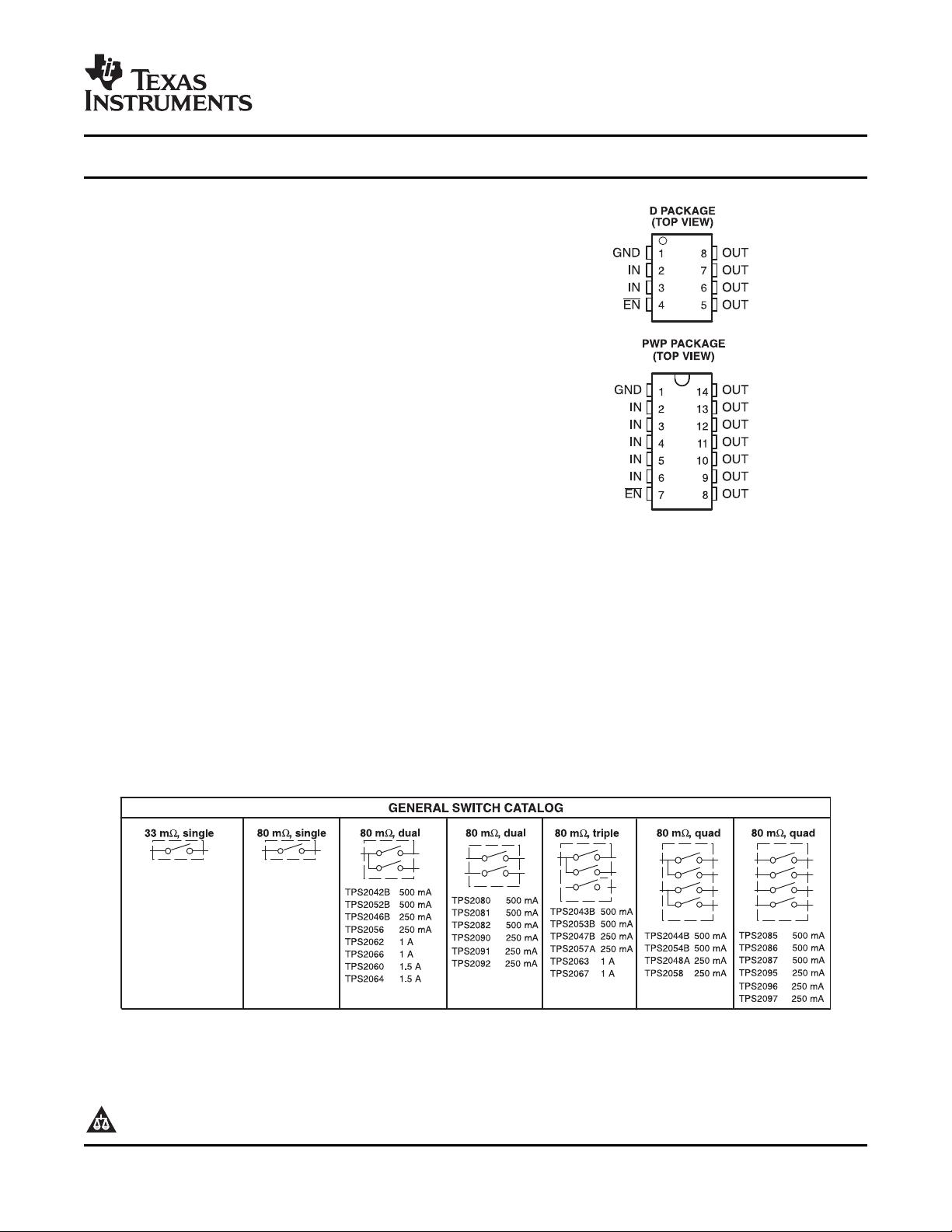
• Available in 8-pin SOIC and 14-Pin TSSOP
Packages
• Ambient Temperature Range, – 40 ° C to 85 ° C
• 2-kV Human-Body-Model, 200-V
Machine-Model ESD Protection
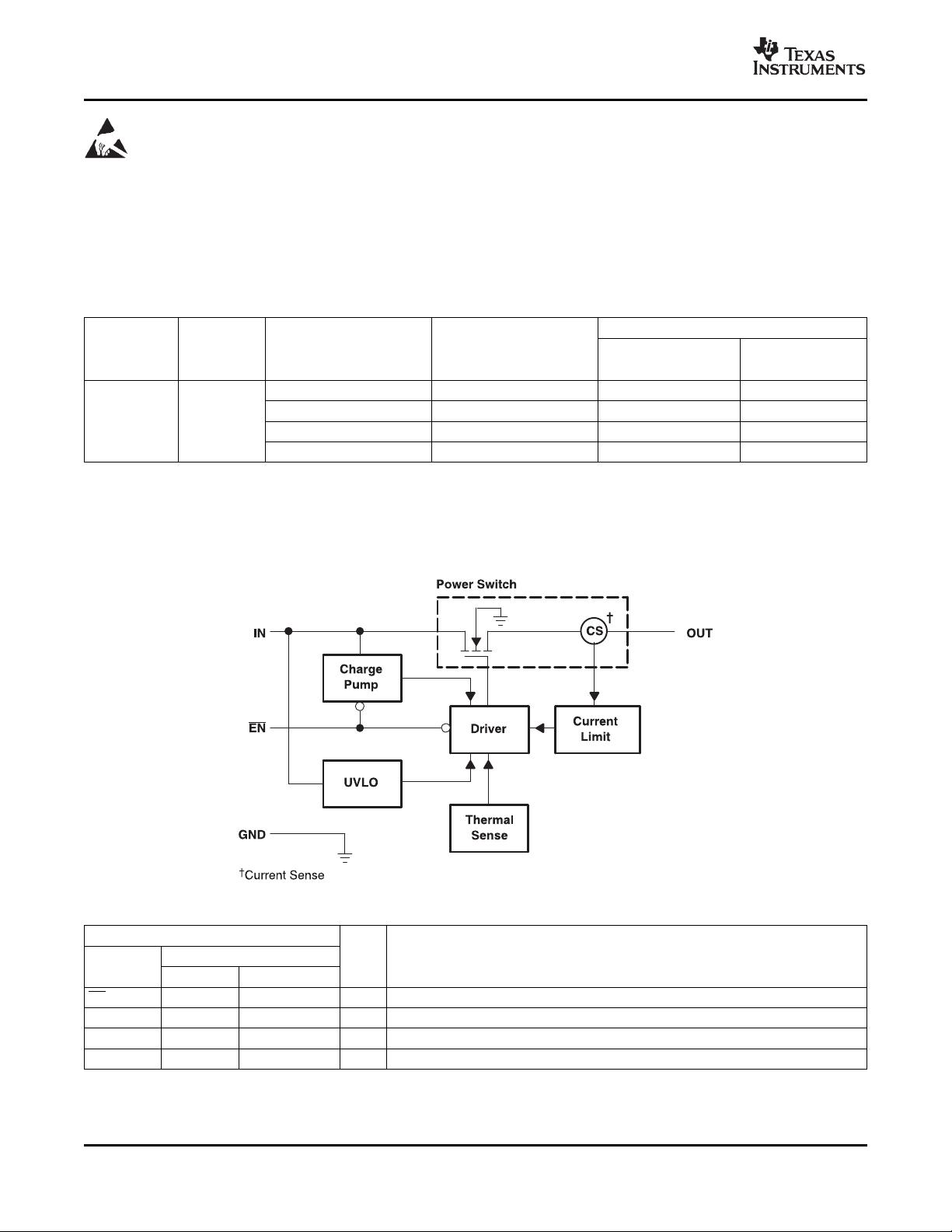
The TPS201xA family of power distribution switches is intended for applications where heavy capacitive loads
and short circuits are likely to be encountered. These devices are 50-m Ω N-channel MOSFET high-side power
switches. The switch is controlled by a logic enable compatible with 5-V logic and 3-V logic. Gate drive is
provided by an internal charge pump designed to control the power-switch rise times and fall times to minimize
current surges during switching. The charge pump requires no external components and allows operation from
supplies as low as 2.7 V.
When the output load exceeds the current-limit threshold or a short is present, the TPS201xA limits the output
current to a safe level by switching into a constant-current mode. When continuous heavy overloads and short
circuits increase the power dissipation in the switch, causing the junction temperature to rise, a thermal
protection circuit shuts off the switch to prevent damage. Recovery from a thermal shutdown is automatic once
the device has cooled sufficiently. Internal circuitry ensures the switch remains off until valid input voltage is
present.
1
Please be aware that an important notice concerning availability, standard warranty, and use in critical applications of
Texas Instruments semiconductor products and disclaimers thereto appears at the end of this data sheet.
PRODUCTION DATA information is current as of publication date.
Copyright © 1998 – 2007, Texas Instruments Incorporated
Products conform to specifications per the terms of the Texas
Instruments standard warranty. Production processing does not
necessarily include testing of all parameters.
www.ti.com
DESCRIPTION (CONTINUED)
TPS201xA FUNCTIONAL BLOCK DIAGRAM
TPS2010A, TPS2011A
TPS2012A, TPS2013A
SLVS189C – DECEMBER 1998 – REVISED SEPTEMBER 2007
These devices have limited built-in ESD protection. The leads should be shorted together or the device placed in conductive foam
during storage or handling to prevent electrostatic damage to the MOS gates.
The TPS201xA devices differ only in short-circuit current threshold. The TPS2010A limits at 0.3-A load, the
TPS2011 at 0.9-A load, the TPS2012A at 1.5-A load, and the TPS2013A at 2.2-A load (see Available Options).
The TPS201xA is available in an 8-pin small-outline integrated-circuit (SOIC) package and in a 14-pin thin-shrink
small-outline package (TSSOP) and operates over a junction temperature range of -40 ° C to 125 ° C.)
AVAILABLE OPTIONS
RECOMMENDED PACKAGED DEVICES
(1)
TYPICAL SHORT-CIRCUIT
MAXIMUM CONTINUOUS
SMALL OUTLINE TSSOP
T
A
ENABLE CURRENT LIMIT AT 25 ° C
LOAD CURRENT
(D)
(2)
(PWP)
(3)
(A)
(A)
0.2 0.3 TPS2010AD TPS2010APWPR
0.6 0.9 TPS2011AD TPS2011APWPR
– 40 ° C to 85 ° C Active low
1 1.5 TPS2012AD TPS2012APWPR
1.5 2.2 TPS2013AD TPS2013APWPR
(1) For the most current package and ordering information, see the Package Option Addendum at the end of this document, or see the TI
website at www.ti.com .
(2) The D package is available taped and reeled. Add an R suffix to device type (e.g., TPS2010DR)
(3) The PWP package is only available left-end taped-and-reeled.
TERMINAL FUNCTIONS
TERMINAL
NO. I/O DESCRIPTION
NAME
D PWP
EN 4 7 I Enable input. Logic low turns on power switch.
GND 1 1 I Ground
IN 2, 3 2 – 6 I Input voltage
OUT 5 – 8 8 – 14 O Power-switch output
2 Submit Documentation Feedback Copyright © 1998 – 2007, Texas Instruments Incorporated
Product Folder Link(s): TPS2010A, TPS2011A TPS2012A, TPS2013A
www.ti.com
DETAILED DESCRIPTION
POWER SWITCH
CHARGE PUMP
DRIVER
ENABLE ( EN)
CURRENT SENSE
THERMAL SENSE
UNDERVOLTAGE LOCKOUT
TPS2010A, TPS2011A
TPS2012A, TPS2013A
SLVS189C – DECEMBER 1998 – REVISED SEPTEMBER 2007
The power switch is an N-channel MOSFET with a maximum on-state resistance of 50 m Ω (V
I(IN)
= 5V).
Configured as a high-side switch, the power switch prevents current flow from OUT to IN and IN to OUT when
disabled.
An internal charge pump supplies power to the driver circuit and provides the necessary voltage to pull the gate
of the MOSFET above the source. The charge pump operates from input voltages as low as 2.7 V and requires
very little supply current.
The driver controls the gate voltage of the power switch. To limit large current surges and reduce the associated
electromagnetic interference (EMI) produced, the driver incorporates circuitry that controls the rise times and fall
times of the output voltage. The rise and fall times are typically in the 2-ms to 9-ms range.
The logic enable disables the power switch, the bias for the charge pump, driver, and other circuitry to reduce the
supply current to less than 10 μ A when a logic high is present on EN . A logic zero input on EN restores bias to
the drive and control circuits and turns the power on. The enable input is compatible with both TTL and CMOS
logic levels.
A sense FET monitors the current supplied to the load. The sense FET measures current more efficiently than
conventional resistance methods. When an overload or short circuit is encountered, the current-sense circuitry
sends a control signal to the driver. The driver, in turn, reduces the gate voltage and drives the power FET into
its saturation region, which switches the output into a constant current mode and holds the current constant while
varying the voltage on the load.
An internal thermal-sense circuit shuts off the power switch when the junction temperature rises to approximately
140 ° C. Hysteresis is built into the thermal sense circuit. After the device has cooled approximately 20 ° C, the
switch turns back on. The switch continues to cycle off and on until the fault is removed.
A voltage sense circuit monitors the input voltage. When the input voltage is below approximately 2 V, a control
signal turns off the power switch.
Copyright © 1998 – 2007, Texas Instruments Incorporated Submit Documentation Feedback 3
Product Folder Link(s): TPS2010A, TPS2011A TPS2012A, TPS2013A
www.ti.com
ABSOLUTE MAXIMUM RATINGS
DISSIPATION RATINGS
RECOMMENDED OPERATING CONDITIONS
TPS2010A, TPS2011A
TPS2012A, TPS2013A
SLVS189C – DECEMBER 1998 – REVISED SEPTEMBER 2007
over operating free-air temperature range (unless otherwise noted)
(1)
VALUE UNIT
V
I(IN)
Input voltage range
(2)
– 0.3 to 6 V
V
O(OUT)
Output voltage range
(2)
– 0.3 to V
I(IN)
+ 0.3 V
V
I(EN)
Input voltage range – 0.3 to 6 V
I
O(OUT)
Continuous output current Internally Limited
Continuous total power dissipation See Dissipation Rating Table
T
J
Operating virtual junction temperature range – 40 to 125 ° C
T
stg
Storage temperature range – 65 to 150 ° C
Lead temperature soldering 1,6 mm (1/16 inch) from case for 10 seconds 260 ° C
Human body model 2 kV
ESD Electrostatic discharge protection
Machine model 200 V
(1) Stresses beyond those listed under absolute maximum ratings may cause permanent damage to the device. These are stress ratings
only, and functional operation of the device at these or any other conditions beyond those indicated under recommended operating
conditions is not implied. Exposure to absolute-maximum-rated conditions for extended periods may affect device reliability.
(2) All voltages are with respect to GND.
T
A
≤ 25 ° C DERATING FACTOR T
A
= 70 ° C T
A
= 85 ° C
PACKAGE
POWER RATING ABOVE T
A
= 25 ° C POWER RATING POWER RATING
D 725 mW 5.8 mW/ ° C 464 mW 377 mW
PWP 700 mW 5.6 mW/ ° C 448 mW 364 mW
over operating free-air temperature range (unless otherwise noted)
MIN MAX UNIT
V
I(IN)
2.7 5.5
Input voltage V
V
IH
0 5.5
TPS2010A 0 0.2
TPS2011A 0 0.6
I
O
Continuous output current A
TPS2012A 0 1
TPS2013A 0 1.5
T
J
Operating virtual junction temperature – 40 125 ° C
4 Submit Documentation Feedback Copyright © 1998 – 2007, Texas Instruments Incorporated
Product Folder Link(s): TPS2010A, TPS2011A TPS2012A, TPS2013A
www.ti.com
ELECTRICAL CHARACTERISTICS
TPS2010A, TPS2011A
TPS2012A, TPS2013A
SLVS189C – DECEMBER 1998 – REVISED SEPTEMBER 2007
over recommended operating junction temperature range, V
I(IN)
= 5.5 V, I
O
= rated current, EN = 0 V (unless otherwise noted)
PARAMETER TEST CONDITIONS
(1)
MIN TYP MAX UNIT
POWER SWITCH
V
I(IN)
= 5 V, T
J
= 25 ° C, I
O
= 1.5 A 33 36
V
I(IN)
= 5 V, T
J
= 85 ° C, I
O
= 1.5 A 38 46
V
I(IN)
= 5 V, T
J
= 125 ° C, I
O
= 1.5 A 44 50
TPS2013A m Ω
V
I(IN)
= 3.3 V, T
J
= 25 ° C, I
O
= 1.5 A 37 41
V
I(IN)
= 3.3 V, T
J
= 85 ° C, I
O
= 1.5 A 43 52
V
I(IN)
= 3.3 V, T
J
= 125 ° C, I
O
= 1.5 A 51 61
Static drain-source on-state
r
DS(on)
resistance
V
I(IN)
= 5 V, T
J
= 25 ° C, I
O
= 0.18 A 30 34
V
I(IN)
= 5 V, T
J
= 85 ° C, I
O
= 0.18 A 35 41
V
I(IN)
= 5 V, T
J
= 125 ° C, I
O
= 0.18 A 39 47
TPS2010A m Ω
V
I(IN)
= 3.3 V, T
J
= 25 ° C, I
O
= 0.18 A 33 37
V
I(IN)
= 3.3 V, T
J
= 85 ° C, I
O
= 0.18 A 39 46
V
I(IN)
= 3.3 V, T
J
= 125 ° C, I
O
= 0.18 A 44 56
V
I(IN)
= 5.5 V, T
J
= 25 ° C, C
L
= 1 μ F, R
L
= 10 Ω 6.1
t
r
Rise time, output ms
V
I(IN)
= 2.7 V, T
J
= 25 ° C, C
L
= 1 μ F, R
L
= 10 Ω 8.6
V
I(IN)
= 5.5 V, T
J
= 25 ° C, C
L
= 1 μ F, R
L
= 10 Ω 3.4
t
f
Rise time, output ms
V
I(IN)
= 2.7 V, T
J
= 25 ° C, C
L
= 1 μ F, R
L
= 10 Ω 3
ENABLE INPUT ( EN)
V
IH
High-level input voltage 2.7 V ≤ V
I(IN)
≤ 5.5 V 2 V
4.5 V ≤ V
I(IN)
≤ 5.5 V 0.8
V
IL
Low-level input voltage V
2.7 V ≤ V
I(IN)
≤ 4.5 V 0.5
I
I
Input current EN = 0 V or EN = V
I(IN)
– 0.5 0.5 μ A
t
on
Turnon time C
L
= 100 μ F, R
L
= 10 Ω 20 ms
t
off
Turnoff time C
L
= 100 μ F, R
L
= 10 Ω 40 ms
CURRENT LIMIT
TPS2010A 0.22 0.3 0.4
T
J
= 25 ° C, V
I
= 5.5 V,
TPS2011A 0.66 0.9 1.1
I
OS
Short-circuit output current OUT connected to GND, A
TPS2012A 1.1 1.5 1.8
Device enable into short circuit
TPS2013A 1.65 2.2 2.7
(1) Pulse-testing techniques maintain junction temperature close to ambient temperature; thermal effects must be taken into account
separately.
Copyright © 1998 – 2007, Texas Instruments Incorporated Submit Documentation Feedback 5
Product Folder Link(s): TPS2010A, TPS2011A TPS2012A, TPS2013A
剩余29页未读,继续阅读
资源评论
不觉明了
- 粉丝: 3175
- 资源: 5443
上传资源 快速赚钱
- 我的内容管理 展开
- 我的资源 快来上传第一个资源
- 我的收益 登录查看自己的收益
- 我的积分 登录查看自己的积分
- 我的C币 登录后查看C币余额
- 我的收藏
- 我的下载
- 下载帮助
安全验证
文档复制为VIP权益,开通VIP直接复制
信息提交成功