TI-TMP141.pdf
需积分: 5 80 浏览量
2023-04-22
16:10:58
上传
评论
收藏 1.02MB PDF 举报

FEATURES
D SensorPath INTERFACE
D FOUR ADDRESSES
D RESOLUTION: +0.25°C (10-bit)
D WIDE TEMPERATURE RANGE:
−40°C to +125°C
D LOW QUIESCENT CURRENT: 110µA (typ)
D TEMPERATURE ACCURACY: ±2°C (max)
D EXTENDED SUPPLY RANGE: +2.7V to +5.5V
D MICRO-SIZE PACKAGES:
SOT23-6 or MSOP-8
APPLICATIONS
D MOTHERBOARDS
D VIDEO CARDS
D BASE STATIONS
D ROUTERS
DESCRIPTION
The TMP141 is a digital output temperature sensor that
utilizes the single-wire SensorPath interface. The TMP141
is capable of measuring temperatures within 2°C of
accuracy over a temperature range of −25°C to +85°C and
3°C of accuracy over −40°C to +125°C. Low supply
current, and a supply range from 2.7V to 5.5V, make the
TMP141 an excellent candidate for a wide range of
low-power applications. The TMP141 is available in
SOT23-6 and MSOP-8 packages.
The TMP141 provides a simple, low-cost way to do
temperature measurement/monitoring and is ideal as a
part of an overall hardware health monitoring system. Up
to four TMP141s can be attached to a SensorPath bus. A
master configures the TMP141s and reads the
temperature output from all devices. No external sensing
components are needed for the TMP141 to measure and
report temperature.
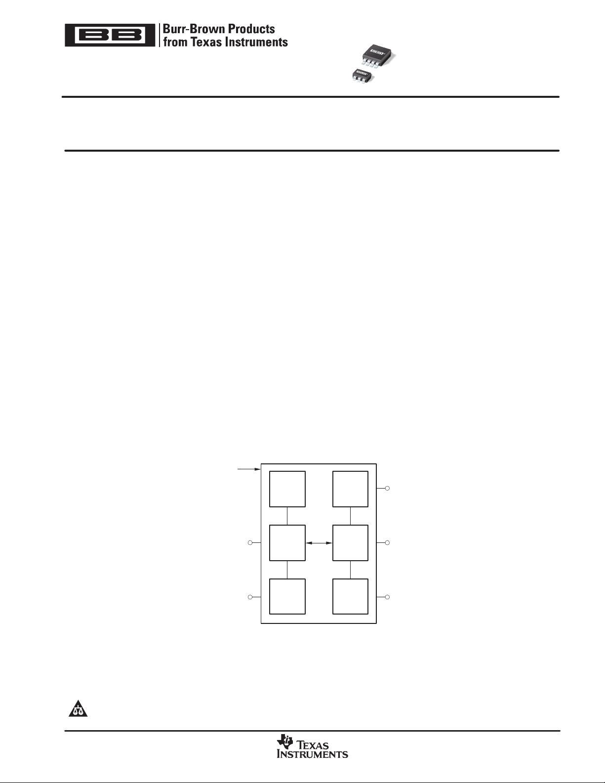
Diode
Te m p .
Sensor
∆Σ
A/D
Converter
OSC
Control
Logic
Serial
Interface
Config.
and Temp.
Register
TMP141
Temperature
V+
GND
ADD0
ADD1
SWD
TMP141
SBAS347A − MARCH 2005 − REVISED JULY 2006
Digital Out Temperature Sensor with
Single-Wire SensorPath Bus
! !
www.ti.com
Copyright 2005−2006, Texas Instruments Incorporated
Please be aware that an important notice concerning availability, standard warranty, and use in critical applications of Texas Instruments
semiconductor products and disclaimers thereto appears at the end of this data sheet.
SensorPath is a trademark of National Semiconductor. All other trademarks are the property of their respective owners.

剩余24页未读,继续阅读
资源评论


