TI-TMP63.pdf
需积分: 5 188 浏览量
2023-04-22
16:10:24
上传
评论 1
收藏 1.59MB PDF 举报

ADVANCEINFORMATION
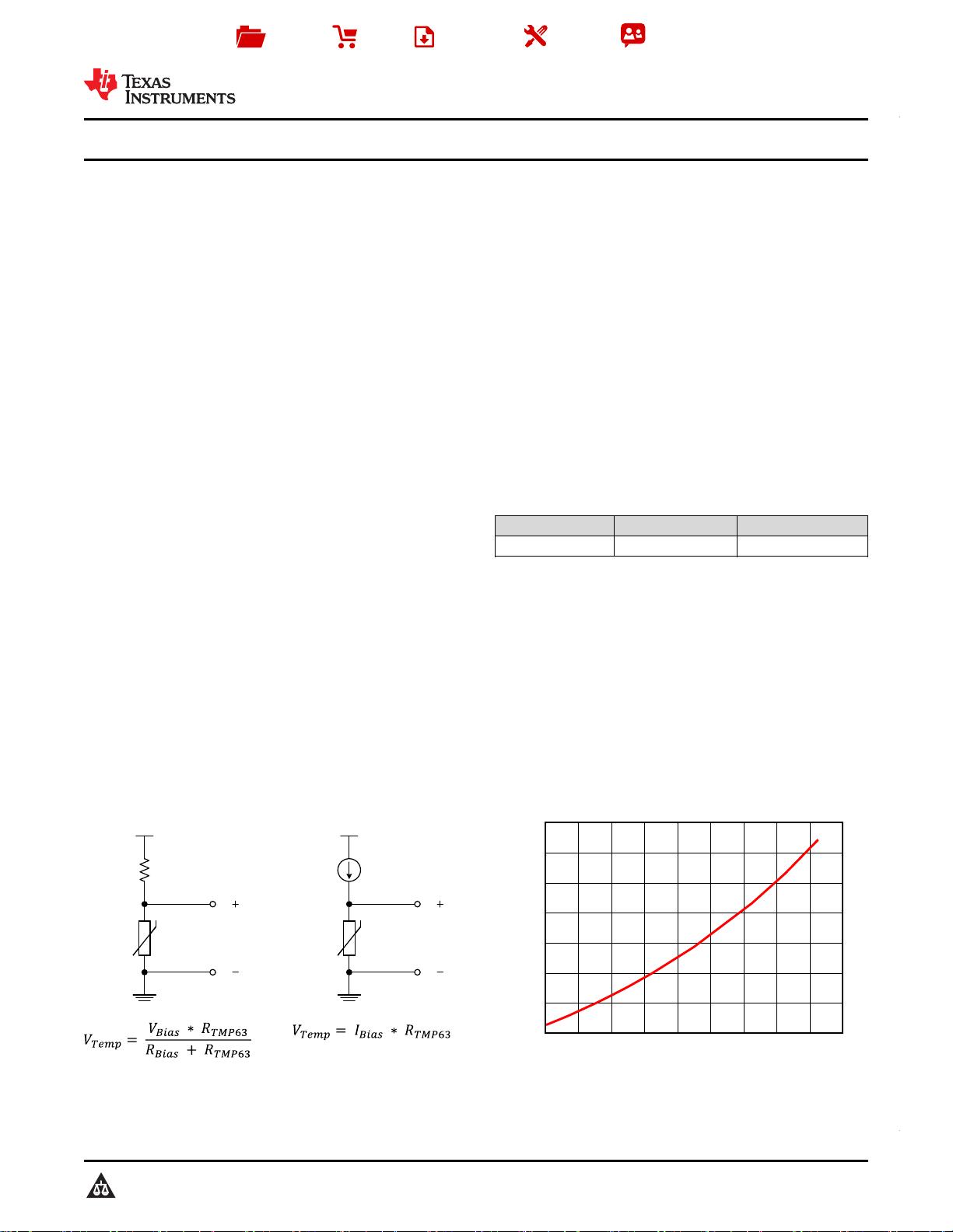
Temperature (qC)
Resistance (k:)
-40 -20 0 20 40 60 80 100 120 140
60
80
100
120
140
160
180
200
TMP6
R
Bias
V
Bias
V
Temp
R
TMP63
V
Temp
R
TMP63
I
Bias
Product
Folder
Order
Now
Technical
Documents
Tools &
Software
Support &
Community
本文档旨在为方便起见,提供有关 TI 产品中文版本的信息,以确认产品的概要。 有关适用的官方英文版本的最新信息,请访问 www.ti.com,其内容始终优先。 TI 不保证翻译的准确
性和有效性。 在实际设计之前,请务必参考最新版本的英文版本。
English Data Sheet: SNIS211
TMP63
ZHCSKB0 –OCTOBER 2019
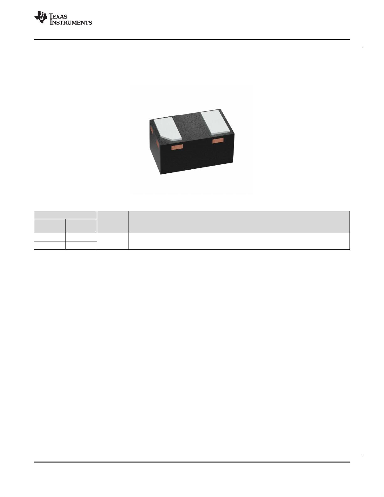
采采用用小小型型 0402 封封装装的的 TMP63 100kΩ 线线性性热热敏敏电电阻阻
1
1 特特性性
1
• 具有
正温度系数 (PTC) 的硅基热敏电阻
• 与非线性热敏电阻相比,线性热敏电阻随温度变化
– 可简化电阻/温度转换方法
– 可降低查找表内存要求
– 无需线性化电路或多点校准
– 可降低在宽温度范围内的精度
• 在 25°C 下具有 100kΩ 标称电阻 (R25)
• 在整个温度范围内具有稳定的灵敏度
– 6400ppm/°C TCR (25°C)
– 在整个温度范围内具有 0.2% 的典型 TCR 容差
(-40°C 至 125°C)
• 宽工作温度范围:
– –40°C 至 125°C
• 快速热响应时间:
– 对于 DEC 封装为 0.6秒
• 长寿命和稳健性能
– 与由于自加热而尽可能降低误差的传统 NTC 相
比,具有超低功耗
– 内置失效防护,能够在发生短路故障时提供保护
– 在高温和高湿度环境下测试后可实现 <1% 的最
大漂移
• 提供的封装选项:
– X1SON(DEC/0402 封装尺寸)
2 应应用用
• 温度测量与监测
• 热补偿
• 热保护(带有比较器)
3 说说明明
TMP63 小型硅线性热敏电阻用于温度测量、保护、补
偿和控制系统。与传统 NTC 热敏电阻相比,TMP63
器件可在整个温度范围内提供增强的线性和一致的灵敏
度。
TMP63 器件具有稳健的性能,这得益于它对环境变化
的抗扰能力和内置的高温下失效防护行为。此器件目前
可采用兼容 0402 尺寸的 2 引脚表面贴装 X1SON 封
装、。
器器件件信信息息
(1)
器器件件型型号号 封封装装 封封装装尺尺寸寸((标标称称值值))
TMP63 X1SON (2) 0.60mm x 1.00mm
(1) 如需了解所有可用封装,请参阅数据表末尾的可订购产品附
录。
空白
空白
空白
空白
空白
空白
典典型型实实施施电电路路 典典型型电电阻阻与与环环境境温温度度间间的的关关系系


剩余25页未读,继续阅读
资源评论


