IPA60R120P7 INFINEON 英飞凌 电子元器件芯片.pdf
需积分: 5 22 浏览量
2023-06-07
11:25:10
上传
评论
收藏 1.06MB PDF 举报

1
IPA60R120P7
Rev.2.1,2018-05-15Final Data Sheet
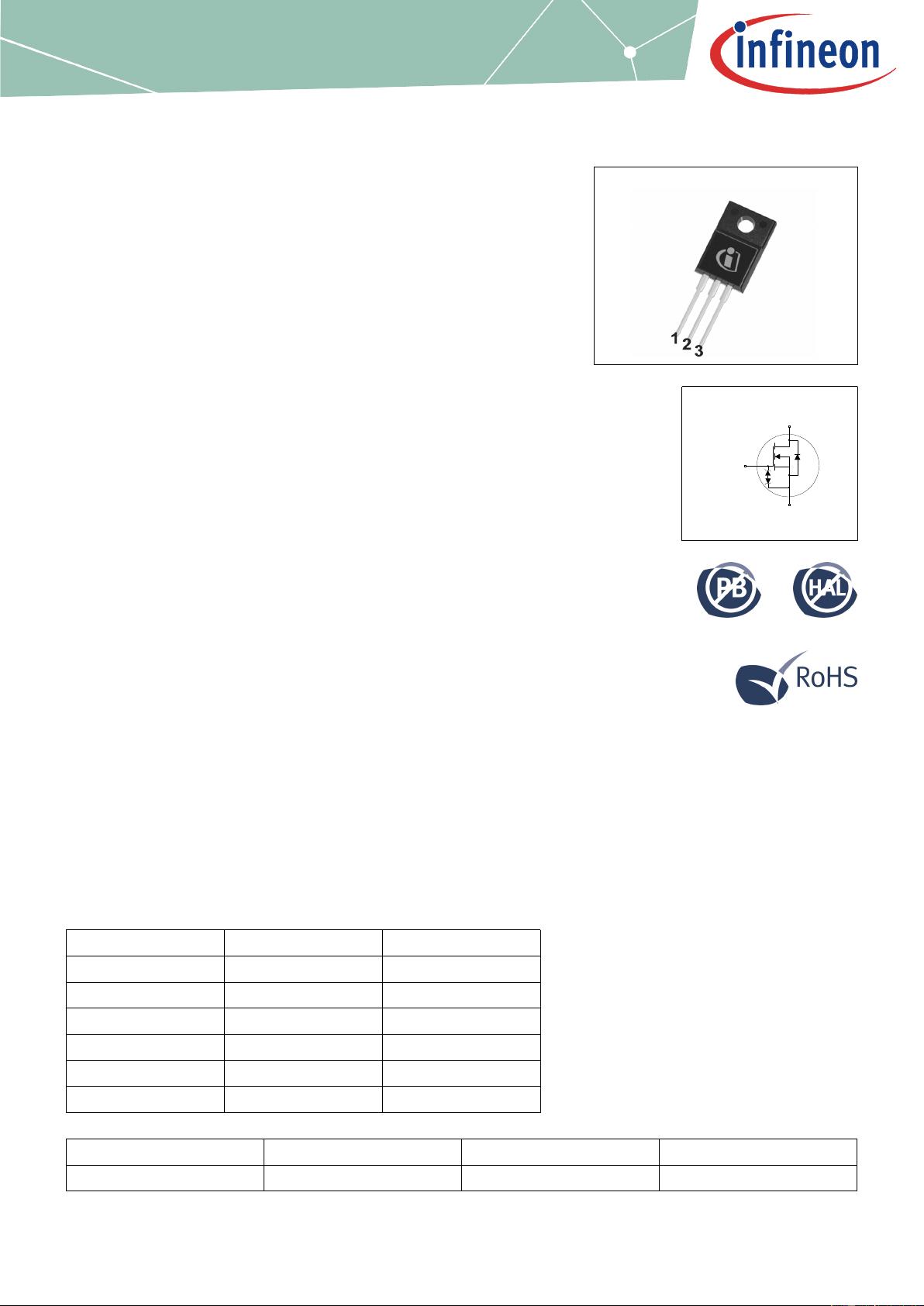
PG-TO220FP
Drain
Pin 2
Gate
Pin 1
Source
Pin 3
MOSFET
600VCoolMOSªP7PowerTransistor
TheCoolMOS™7thgenerationplatformisarevolutionarytechnologyfor
highvoltagepowerMOSFETs,designedaccordingtothesuperjunction
(SJ)principleandpioneeredbyInfineonTechnologies.The600V
CoolMOS™P7seriesisthesuccessortotheCoolMOS™P6series.It
combinesthebenefitsofafastswitchingSJMOSFETwithexcellentease
ofuse,e.g.verylowringingtendency,outstandingrobustnessofbody
diodeagainsthardcommutationandexcellentESDcapability.
Furthermore,extremelylowswitchingandconductionlossesmake
switchingapplicationsevenmoreefficient,morecompactandmuch
cooler.
Features
•Suitableforhardandsoftswitching(PFCandLLC)duetoanoutstanding
commutationruggedness
•Significantreductionofswitchingandconductionlosses
•ExcellentESDrobustness>2kV(HBM)forallproducts
•BetterR
DS(on)
/packageproductscomparedtocompetitionenabledbya
lowR
DS(on)
*A(below1Ohm*mm²)
•Fullyqualifiedacc.JEDECforIndustrialApplications
Benefits
•Easeofuseandfastdesign-inthroughlowringingtendencyandusage
acrossPFCandPWMstages
•Simplifiedthermalmanagementduetolowswitchingandconduction
losses
•Increasedpowerdensitysolutionsenabledbyusingproductswith
smallerfootprintandhighermanufacturingqualitydueto>2kVESD
protection
•Suitableforawidevarietyofapplicationsandpowerranges
Potentialapplications
PFCstages,hardswitchingPWMstagesandresonantswitchingstages
fore.g.PCSilverbox,Adapter,LCD&PDPTV,Lighting,Server,Telecom
andUPS.
Pleasenote:ForMOSFETparallelingtheuseofferritebeadsonthegate
orseparatetotempolesisgenerallyrecommended.
Table1KeyPerformanceParameters
Parameter Value Unit
V
DS
@ T
j,max
650 V
R
DS(on),max
120 mΩ
Q
g,typ
36 nC
I
D,pulse
78 A
E
oss
@ 400V 4.0 µJ
Body diode di
F
/dt 900 A/µs
Type/OrderingCode Package Marking RelatedLinks
IPA60R120P7 PG-TO 220 FullPAK 60R120P7 see Appendix A


剩余13页未读,继续阅读
资源评论


