AUIRF7737L2TR INFINEON 英飞凌 电子元器件芯片.pdf
需积分: 5 107 浏览量
2023-05-27
12:31:38
上传
评论
收藏 293KB PDF 举报

www.irf.com 1
AUIRF7737L2TR
AUIRF7737L2TR1
AUTOMOTIVE GRADE
HEXFET
®
is a registered trademark of International Rectifier.
11/08/10
Description
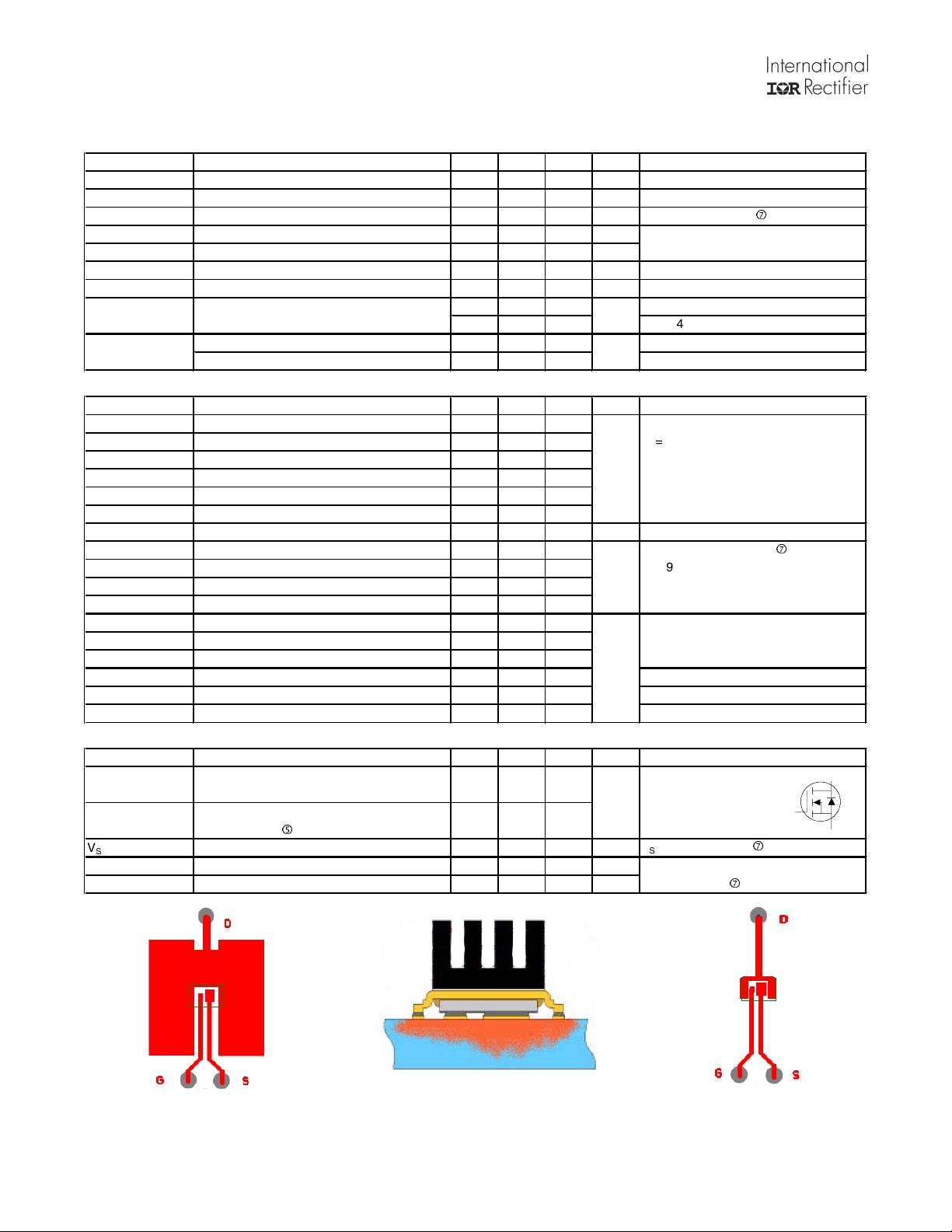
The AUIRF7737L2 combines the latest Automotive HEXFET® Power MOSFET Silicon technology with the advanced DirectFET® packaging
technology to achieve exceptional performance in a package that has the footprint of a DPak (TO-252AA) and only 0.7 mm profile. The
DirectFET® package is compatible with existing layout geometries used in power applications, PCB assembly equipment and vapor phase, infra-
red or convection soldering techniques, when application note AN-1035 is followed regarding the manufacturing methods and processes. The
DirectFET® package allows dual sided cooling to maximize thermal transfer in automotive power systems.
This HEXFET® Power MOSFET is designed for applications where efficiency and power density are of value. The advanced DirectFET® packaging
platform coupled with the latest silicon technology allows the AUIRF7737L2 to offer substantial system level savings and performance improvement
specifically in motor drive, high frequency DC-DC and other heavy load applications on ICE, HEV and EV platforms. This MOSFET utilizes the latest
processing techniques to achieve low on-resistance and low Qg per silicon area. Additional features of this MOSFET are 175°C operating junction
temperature and high repetitive peak current capability. These features combine to make this MOSFET a highly efficient, robust and reliable
device for high current automotive applications.
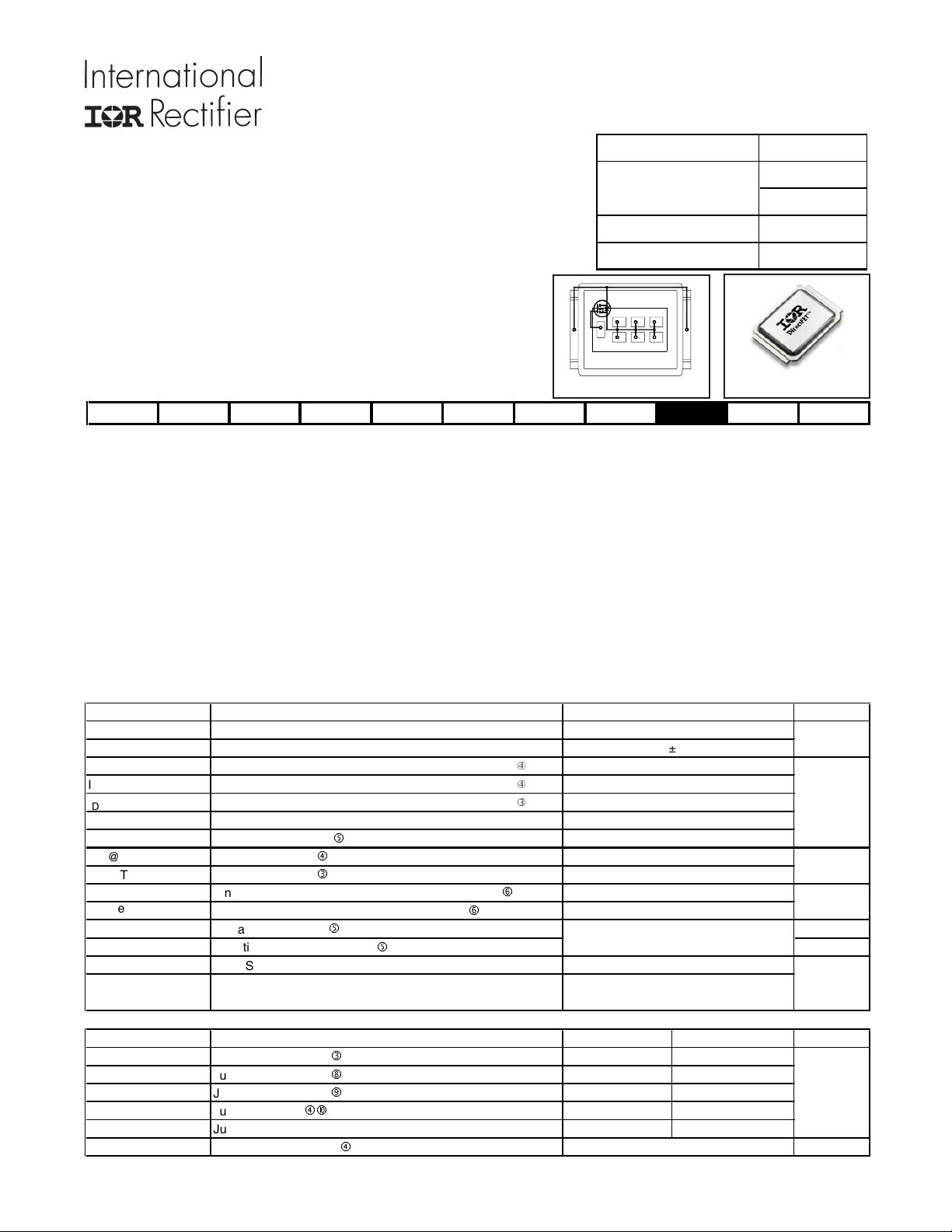
Applicable DirectFET
®
Outline and Substrate Outline
DirectFET
®
ISOMETRIC
L6
SB SC M2 M4 L4 L6 L8
DD
G
S
S
S
S
S
S
V
(BR)DSS
40V
R
DS(on)
typ.
1.5m
Ω
max.
1.9m
Ω
I
D (Silicon Limited)
156A
Q
g
89nC
• Advanced Process Technology
• Optimized for Automotive Motor Drive, DC-DC and
other Heavy Load Applications
• Exceptionally Small Footprint and Low Profile
• High Power Density
• Low Parasitic Parameters
• Dual Sided Cooling
• 175°C Operating Temperature
• Repetitive Avalanche Capability for Robustness and
Reliability
• Lead Free, RoHS Compliant and Halogen Free
• Automotive Qualified *
Absolute Maximum Ratings
Stresses beyond those listed under “Absolute Maximum Ratings” may cause permanent damage to the device. These are stress ratings only; and
functional operation of the device at these or any other condition beyond those indicated in the specifications is not implied.Exposure to absolute-
maximum-rated conditions for extended periods may affect device reliability. The thermal resistance and power dissipation ratings are measured
under board mounted and still air conditions. Ambient temperature (T
A
) is 25°C, unless otherwise specified.
Parameter Units
V
DS
Drain-to-Source Voltage
V
GS
Gate-to-Source Voltage
I
D
@ T
C
= 25°C
Continuous Drain Current, V
GS
@ 10V (Silicon Limited)
f
I
D
@ T
C
= 100°C
Continuous Drain Current, V
GS
@ 10V (Silicon Limited)
f
I
D
@ T
A
= 25°C
Continuous Drain Current, V
GS
@ 10V (Silicon Limited)
e
I
D
@ T
C
= 25°C Continuous Drain Current, V
GS
@ 10V (Package Limited)
I
DM
Pulsed Drain Current
g
P
D
@T
C
= 25°C Power Dissipation
f
P
D
@T
A
= 25°C Power Dissipation
e
E
AS
Single Pulse Avalanche Energy (Thermally Limited)
h
E
AS
(tested)
Single Pulse Avalanche Energy Tested Value
h
I
AR
Avalanche Current
g
A
E
AR
Repetitive Avalanche Energy
g
mJ
T
P
Peak Soldering Temperature
T
J
Operating Junction and
T
STG
Storage Temperature Range
Thermal Resistance
Parameter Typ. Max. Units
R
θJA
Junction-to-Ambient
e
––– 45
R
θJA
Junction-to-Ambient
j
12.5 –––
R
θJA
Junction-to-Ambient
k
20 –––
R
θJCan
Junction-to-Can
fl
––– 1.8
R
θJ-PCB
Junction-to-PCB Mounted ––– 0.5
Linear Derating Factor
f
W/°C
V
A
mJ
°C/W
W
°C
± 20
315
0.56
31
83
3.3
270
-55 to + 175
Max.
156
110
624
386
104
See Fig.18a, 18b, 16, 17
40
Automotive DirectFET
®
Power MOSFET
PD - 96315C
剩余10页未读,继续阅读
资源评论


芯脉芯城
- 粉丝: 3
- 资源: 4031


最新资源
- 毕业项目:网上图书订阅管理系统的设计与开发(ASP.NET技术+程序源代码+毕业文档)
- zjk-1.ipynb
- Delphi 12 控件之EhLib.v10.2.42 for Delphi 5-12.src.rar
- cloudreve3.8.3的docker镜像
- RB108A-SOT23-5封装 单节锂电池保护IC 深圳市可芯电子有限公司.pdf
- Apache Maven的安装与配置.pdf
- 2024高质量PS练习教程,全程干货无废话
- TPLINK TL-NVR6116K-L 升级包
- RB301A-SOT23-5 单节锂电池保护IC 深圳市可芯电子有限公司.pdf
- scrt-x64-bsafe.9.5.2.3325.exe
资源上传下载、课程学习等过程中有任何疑问或建议,欢迎提出宝贵意见哦~我们会及时处理!
点击此处反馈


