AUIRF7739L2 INFINEON 英飞凌 电子元器件芯片.pdf
需积分: 5 41 浏览量
2023-05-27
12:30:11
上传
评论
收藏 534KB PDF 举报

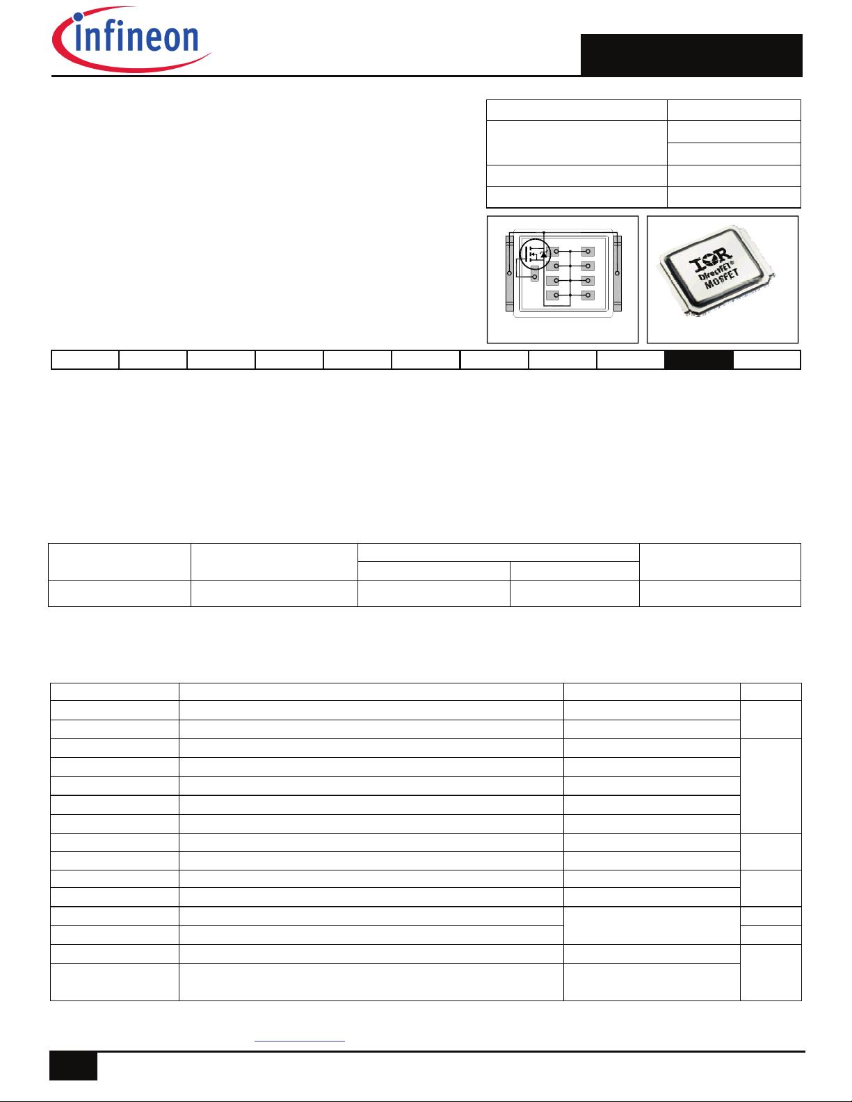
AUIRF7739L2TR
Base Part Number Package Type
Standard Pack
Form Quantity
AUIRF7739L2
DirectFET Large Can
Tape and Reel 4000
AUIRF7739L2TR
Orderable Part Number
AUTOMOTIVE GRADE
V
(BR)DSS
40V
R
DS(on)
typ.
700µ
I
D (Silicon Limited)
270A
max.
1000µ
Q
g (typical)
220nC
DirectFET
®
ISOMETRIC
L8
Automotive DirectFET
®
Power MOSFET
Applicable DirectFET
®
Outline and Substrate Outline
SB SC M2 M4 L4 L6 L8
Description
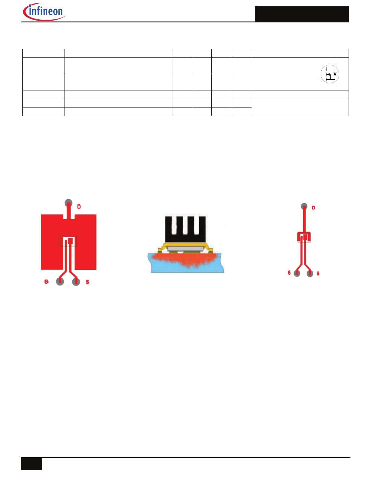
The AUIRF7739L2TR combines the latest Automotive HEXFET® Power MOSFET Silicon technology with the advanced DirectFET® packaging to
achieve the lowest on-state resistance in a package that has the footprint of a DPak (TO-252AA) and only 0.7 mm profile. The DirectFET package is
compatible with existing layout geometries used in power applications, PCB assembly equipment and vapor phase, infra-red or convection soldering
techniques, when application note AN-1035 is followed regarding the manufacturing methods and processes. The DirectFET package allows dual
sided cooling to maximize thermal transfer in automotive power systems.
This HEXFET® Power MOSFET is designed for applications where efficiency and power density are essential. The advanced DirectFET® packaging
platform coupled with the latest silicon technology allows the AUIRF7739L2TR to offer substantial system level savings and performance improvement
specifically in motor drive, high frequency DC-DC and other heavy load applications on ICE, HEV and EV platforms. This MOSFET utilizes the latest
processing techniques to achieve low on-resistance and low Qg per silicon area. Additional features of this MOSFET are 175°C operating junction
temperature and high repetitive peak current capability. These features combine to make this MOSFET a highly efficient, robust and reliable device for
high current automotive applications.
Absolute Maximum Ratings
Stresses beyond those listed under “Absolute Maximum Ratings” may cause permanent damage to the device. These are stress ratings only; and
functional operation of the device at these or any other condition beyond those indicated in the specifications is not implied. Exposure to absolute-
maximum-rated conditions for extended periods may affect device reliability. The thermal resistance and power dissipation ratings are measured under
board mounted and still air conditions. Ambient temperature (TA) is 25°C, unless otherwise specified.
Parameter Max. Units
V
DS
Drain-to-Source Voltage 40
V
V
GS
Gate-to-Source Voltage ±20
I
D
@ T
C
= 25°C Continuous Drain Current, V
GS
@ 10V (Silicon Limited) 270
A
I
D
@ T
C
= 100°C Continuous Drain Current, V
GS
@ 10V (Silicon Limited) 190
I
D
@ T
A
= 25°C Continuous Drain Current, V
GS
@ 10V (Silicon Limited) 46
I
D
@ T
C
= 25°C Continuous Drain Current, V
GS
@ 10V (Package Limited) 375
I
DM
Pulsed Drain Current 1070
P
D
@T
C
= 25°C Power Dissipation 125
W
P
D
@T
A
= 25°C Power Dissipation 3.8
E
AS
Single Pulse Avalanche Energy (Thermally Limited) 270
E
AS (tested)
Single Pulse Avalanche Energy (Tested Value) 160
I
AR
Avalanche Current
See Fig. 16, 17, 18a, 18b
A
E
AR
Repetitive Avalanche Energy
mJ
T
P
Peak Soldering Temperature 270
°C
T
J
Operating Junction and -55 to + 175
T
STG
Storage Temperature Range
mJ
1 2015-11-19
HEXFET® is a registered trademark of Infineon.
*Qualification standards can be found at www.infineon.com
Advanced Process Technology
Optimized for Automotive Motor Drive, DC-DC and
other Heavy Load Applications
Exceptionally Small Footprint and Low Profile
High Power Density
Low Parasitic Parameters
Dual Sided Cooling
175°C Operating Temperature
Repetitive Avalanche Capability for Robustness and Reliability
Lead free, RoHS and Halogen free
Automotive Qualified *
D D
S
S
SS
S
S
S
S
G
剩余10页未读,继续阅读
资源评论


芯脉芯城
- 粉丝: 3
- 资源: 4031


最新资源
- 华为HCIA-WLAN 3.0 课程视频(45 STA无法上线故障排查.mp4)
- 华为HCIA-WLAN 3.0 课程视频(44 AP无法上线故障排查(下).mp4)
- 华为HCIA-WLAN 3.0 课程视频(43 AP无法上线故障排查(上).mp4)
- python实现基于U-net和MRI图像的膀胱壁边缘以及膀胱肿瘤检测(高准确率)+源码+开发文档+模型训练(毕业设计&课程设计
- 华为HCIA-WLAN 3.0 课程视频(42 WLAN系统维护的方法及故障处理命令.mp4)
- 华为HCIA-WLAN 3.0 课程视频(41 WLAN故障处理一般流程(下).mp4)
- C++基于OpenCV+Qt的人脸识别考勤系统-毕业设计+源代码+文档说明.zip
- python爬虫资源下载
- 华为HCIA-WLAN 3.0 课程视频(40 WLAN故障处理一般流程(上).mp4)
- PHP教材管理系统设计(源码+数据库)
资源上传下载、课程学习等过程中有任何疑问或建议,欢迎提出宝贵意见哦~我们会及时处理!
点击此处反馈


