IRFH7084 INFINEON 英飞凌 电子元器件芯片.pdf
需积分: 5 149 浏览量
2023-05-27
12:30:58
上传
评论
收藏 748KB PDF 举报

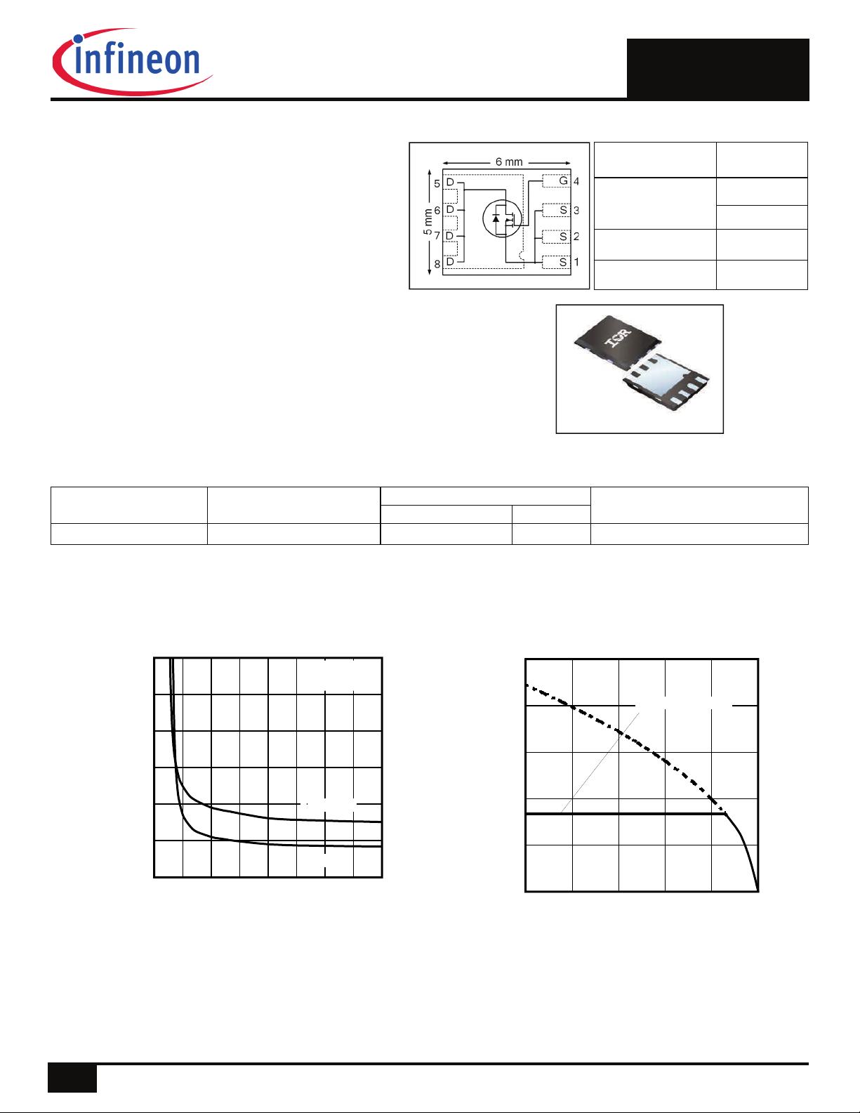
StrongIRFET™
IRFH7084PbF
HEXFET
®
Power MOSFET
Application
Half-bridge and full-bridge topologies
Synchronous rectifier applications
Resonant mode power supplies
DC/DC converters
DC/AC Inverters
Benefits
Improved Gate, Avalanche and Dynamic dV/dt Ruggedness
Fully Characterized Capacitance and Avalanche SOA
Enhanced body diode dV/dt and dI/dt Capability
Lead-Free, RoHS Compliant
V
DSS
40V
R
DS(on) typ.
0.95m
max
1.25m
I
D (Silicon Limited)
265A
I
D (Package Limited)
100A
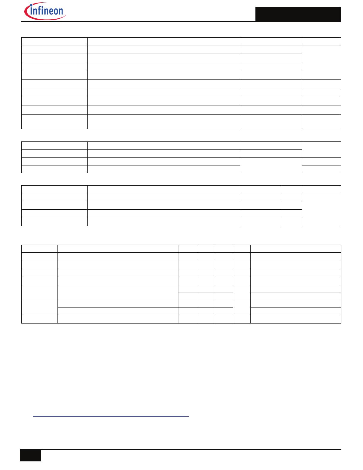
Fig 1. Typical On-Resistance vs. Gate Voltage
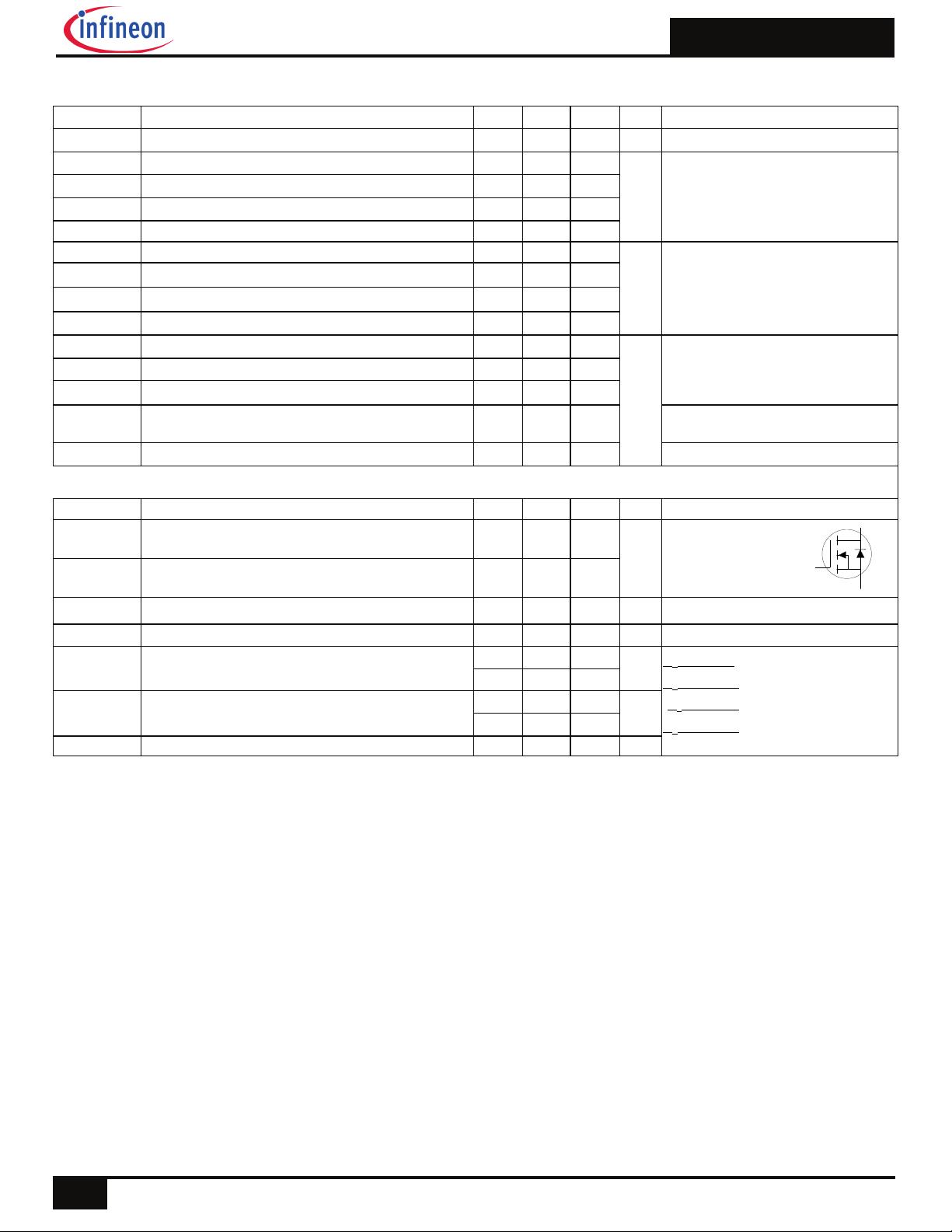
Fig 2. Maximum Drain Current vs. Case Temperature
PQFN 5X6 mm
Base part number Package Type
Standard Pack
Form Quantity
IRFH7084PbF PQFN 5mm x 6mm
Tape and Reel 4000 IRFH7084TRPbF
Orderable Part Number
25 50 75 100 125 150
T
C
, Case Temperature (°C)
0
60
120
180
240
300
I
D
,
D
r
a
i
n
C
u
r
r
e
n
t
(
A
)
Limited by package
4 8 12 16 20
V
GS
, Gate-to-Source Voltage (V)
0
1
2
3
4
5
6
R
D
S
(
o
n
)
,
D
r
a
i
n
-
t
o
-
S
o
u
r
c
e
O
n
R
e
s
i
s
t
a
n
c
e
(
m
)
T
J
= 25°C
T
J
= 125°C
I
D
= 100A
1
2017-01-24
剩余11页未读,继续阅读
资源评论


芯脉芯城
- 粉丝: 3
- 资源: 4031


最新资源
- ParaStor300S 对象存储服务接口参考V1.0(V4.0.X).pdf
- ParaStor300S产品FAQ.doc
- SBM模型、超效率SBM模型代码(原始面板数据、MATLAB)
- 基于汇川AM系列PLC做的CNC加工
- ParaStor300S技术培训PPT-面向售前-V1.4.pptx
- 在MATLAB中,你可以使用多种函数和工具来创建各种类型的图形 以下是一些基本的MATLAB绘图命令和示例:
- 1_网络2204班 30 王磊 open flow 协议分析实践.docx
- 探索 v-on 之奥秘二:事件及各类修饰符的深度剖析与案例展示
- k8s基础教程与相关面试
- TerraScan中文用户指南
资源上传下载、课程学习等过程中有任何疑问或建议,欢迎提出宝贵意见哦~我们会及时处理!
点击此处反馈


