没有合适的资源?快使用搜索试试~ 我知道了~
TI-PCA9548A.pdf
需积分: 9 3 下载量 61 浏览量
2023-02-08
20:47:19
上传
评论 4
收藏 3.24MB PDF 举报
温馨提示
试读
42页
I2C开关
资源推荐
资源详情
资源评论
支持复位的 PCA9548A 低电压 8 通道 I
2
C 开关
1 特性
• 8 选 1 双向转换开关
• 与 I
2
C 总线和系统管理总线 (SMBus) 兼容
• 低电平有效复位输入
• 三个硬件地址引脚允许在 I2C 总线上使用多达八个
PCA9548A 器件
• 通过 I2C 总线实现通道选择
• 加电时所有开关通道取消选定
• 低 R
ON
开关
• 支持 1.8V、2.5V、3.3V 和 5V 总线间的电压电平转
换
• 加电时无干扰
• 支持热插入
• 低待机电流
• 工作电源电压范围为 2.3V 至 5.5V
• 5V 耐压输入
• 0kHz 至 400kHz 时钟频率
• 闩锁性能超过 100mA,符合 JESD 78 II 类规范的
要求
• ESD 保护性能超过 JESD 22 规范要求
– 2000V 人体放电模型 (A114-A)
– 200V 机器放电模型 (A115-A)
– 1000V 带电器件模型 (C101)
2 应用
• 服务器
• 路由器(电信交换设备)
• 工厂自动化
• 具有 I
2
C 从地址冲突的产品(例如,多个完全一样
的温度传感器)
3 说明
PCA9548A 器件配有八个可通过 I2C 总线控制的双向
转换开关。SCL/SDA 上行对扩展到八个下行对,或者
通道。根据可编程控制寄存器的内容,可选择任一单独
的 SCx/SDx 通道或者通道组合。这些下游通道可用于
解决 I
2
C 从器件地址冲突。例如,如果应用中需要八个
完全相同的数字温度传感器,则每个通道 (0-7) 可以连
接一个传感器。
发生超时或其他不当操作时,系统主控器可通过将
RESET 输入置为低电平来复位 PCA9548A。同样,上
电复位即可取消选中所有通道并初始化 I2C/SMBus 状
态机。将 RESET 置为有效也可实现复位和初始化,并
且无需将部件断电。这样可以在下游 I
2
C 总线卡在低电
平状态时进行恢复。
由于开关上有导通栅极,因此 VCC 引脚可用于限制将
由 PCA9548A 传递的最大电压。这样就可以在每个对
上使用不同的总线电压,从而让 1.8V、2.5V 或 3.3V
部件能够在没有任何额外保护的情况下与 5V 部件通
信。对于每个通道,外部上拉电阻器将总线电压上拉至
所需的电压水平。所有 I/O 引脚均可承受 5V 电压。
器件信息
器件名称
封装
(1)
封装尺寸(标称值)
PCA9548A
SSOP (24) 8.20mm × 5.30mm
TVSOP (24) 5.00mm × 4.40mm
SOIC (24) 15.40mm × 7.50mm
TSSOP (24) 7.80mm × 4.40mm
VQFN (24) 4.00mm × 4.00mm
(1) 如需了解所有可用封装,请参阅数据表末尾的可订购产品附
录。
PCA9548A
Slaves A0, A1...AN
Slaves B0, B1...BN
Slaves H0, H1...HN
I2C or SMBus
Master
(processor)
SDA
SCL
SD0
SC0
Channel 0
Channel 1
Channel 7
RESET
SD1
SC1
SD7
SC7
VCC
A1
A2
GND
A0
Slaves C0, C1...CN
Channel 2
SD2
SC2
简化版原理图
PCA9548A
ZHCSJK4G – JUNE 2009 – REVISED MARCH 2021
本文档旨在为方便起见,提供有关 TI 产品中文版本的信息,以确认产品的概要。有关适用的官方英文版本的最新信息,请访问
www.ti.com,其内容始终优先。TI 不保证翻译的准确性和有效性。在实际设计之前,请务必参考最新版本的英文版本。
English Data Sheet: SCPS143
Table of Contents
1 特性................................................................................... 1
2 应用................................................................................... 1
3 说明................................................................................... 1
4 Revision History.............................................................. 2
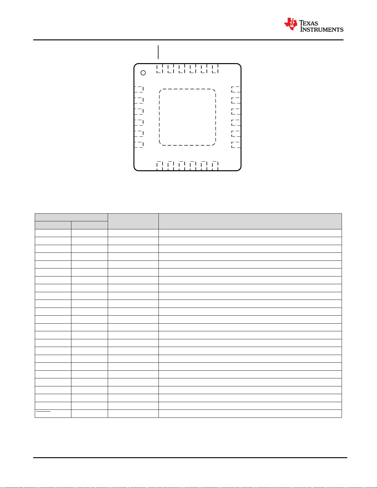
5 Pin Configuration and Functions...................................3
6 Specifications.................................................................. 5
6.1 Absolute Maximum Ratings........................................ 5
6.2 ESD Ratings............................................................... 5
6.3 Recommended Operating Conditions.........................5
6.4 Thermal Information....................................................5
6.5 Electrical Characteristics.............................................6
6.6 I
2
C Interface Timing Requirements.............................8
6.7 Reset Timing Requirements........................................9
6.8 Switching Characteristics............................................9
6.9 Typical Characteristics.............................................. 10
7 Parameter Measurement Information.......................... 11
8 Detailed Description......................................................13
8.1 Overview................................................................... 13
8.2 Functional Block Diagram......................................... 14
8.3 Feature Description...................................................14
8.4 Device Functional Modes..........................................15
8.5 Programming............................................................ 15
8.6 Register Maps...........................................................16
9 Application Information Disclaimer............................. 20
9.1 Application Information............................................. 20
9.2 Typical Application.................................................... 20
10 Power Supply Recommendations..............................24
10.1 Power-On Reset Requirements.............................. 24
11 Layout........................................................................... 26
11.1 Layout Guidelines................................................... 26
11.2 Layout Example...................................................... 27
12 Device and Documentation Support..........................28
12.1 Related Documentation.......................................... 28
12.2 Receiving Notification of Documentation Updates..28
12.3 Support Resources................................................. 28
12.4 Trademarks............................................................. 28
12.5 Electrostatic Discharge Caution..............................28
12.6 Glossary..................................................................28
13 Mechanical, Packaging, and Orderable
Information.................................................................... 28
4 Revision History
注:以前版本的页码可能与当前版本的页码不同
Changes from Revision F (April 2019) to Revision G (March 2021) Page
• Changed the PW and RGE package values in the Thermal Information. ..........................................................5
• Changed the V
PORR
row in the Electrical Characteristics .................................................................................. 6
• Added V
PORF
row to the Electrical Characteristics ............................................................................................ 6
• Changed the I
CC
Low inputs and High inputs values in the Electrical Characteristics .......................................6
• Changed the Power Supply Recommendations .............................................................................................. 24
Changes from Revision E (February 2015) to Revision F (April 2019) Page
• 更新了
节
3 部分.................................................................................................................................................. 1
• Changed the Pin Configuration images.............................................................................................................. 3
• Updated Pin Name for Pin 8 From: SC2 To: SD2 in the Pin Functions table..................................................... 3
• Added the Typical Characteristics section........................................................................................................ 10
Changes from Revision D (June 2014) to Revision E (February 2015) Page
• 更改了首页图...................................................................................................................................................... 1
• Added Thermal Information. .............................................................................................................................. 5
• Changed Note
(2)
in the Electrical Characteristics ............................................................................................. 6
• Added Layout Example.....................................................................................................................................27
Changes from Revision C (June 2007) to Revision D (June 2014) Page
• Added RESET Errata section........................................................................................................................... 15
• Updated Typical Application schematic. .......................................................................................................... 20
PCA9548A
ZHCSJK4G – JUNE 2009 – REVISED MARCH 2021
www.ti.com.cn
2 Submit Document Feedback
Copyright © 2021 Texas Instruments Incorporated
Product Folder Links: PCA9548A
5 Pin Configuration and Functions
1A0 24
V
CC
2A1 23 SDA
3RE SET 22 SCL
4SD0 21 A2
5SC0 20 SC7
6SD1 19 SD7
7SC1 18 SC6
8SD2 17 SD6
9SC2 16 SC5
10SD3 15 SD5
11SC3 14 SC4
12GND 13 SD4
No t to scale
图 5-1. DB, DGV, DW or PW Package, 24-Pin SSOP, TVSOP, SOIC or TSSOP , Top View
表 5-1. Pin Functions
PIN
I/O DESCRIPTION
NAME
NO.
DB, DW, DGV ,
PW
A0 1 I Address input 0. Connect directly to V
CC
or ground
A1 2 I Address input 1. Connect directly to V
CC
or ground
RESET 3 I Active-low reset input. Connect to V
CC
through a pull-up resistor, if not used
SD0 4 I/O Serial data 0. Connect to V
CC
through a pull-up resistor
SC0 5 I/O Serial clock 0. Connect to V
CC
through a pull-up resistor
SD1 6 I/O Serial data 1. Connect to V
CC
through a pull-up resistor
SC1 7 I/O Serial clock 1. Connect to V
CC
through a pull-up resistor
SD2 8 I/O Serial data 2. Connect to V
CC
through a pull-up resistor
SC2 9 I/O Serial clock 2. Connect to V
CC
through a pull-up resistor
SD3 10 I/O Serial data 3. Connect to V
CC
through a pull-up resistor
SC3 11 I/O Serial clock 3. Connect to V
CC
through a pull-up resistor
GND 12
—
Ground
SD4 13 I/O Serial data 4. Connect to V
CC
through a pull-up resistor
SC4 14 I/O Serial clock 4. Connect to V
CC
through a pull-up resistor
SD5 15 I/O Serial data 5. Connect to V
CC
through a pull-up resistor
SC5 16 I/O Serial clock 5. Connect to V
CC
through a pull-up resistor
SD6 17 I/O Serial data 6. Connect to V
CC
through a pull-up resistor
SC6 18 I/O Serial clock 6. Connect to V
CC
through a pull-up resistor
SD7 19 I/O Serial data 7. Connect to V
CC
through a pull-up resistor
SC7 20 I/O Serial clock 7. Connect to V
CC
through a pull-up resistor
A2 21 I Address input 2. Connect directly to V
CC
or ground
SCL 22 I/O Serial clock bus. Connect to V
CC
through a pull-up resistor
SDA 23 I/O Serial data bus. Connect to V
CC
through a pull-up resistor
V
CC
24
—
Supply voltage
www.ti.com.cn
PCA9548A
ZHCSJK4G – JUNE 2009 – REVISED MARCH 2021
Copyright © 2021 Texas Instruments Incorporated
Submit Document Feedback
3
Product Folder Links: PCA9548A
24 RE SET7SD3
1SD0 18 A2
23 A18SC3
2SC0 17 SC7
22 A09GND
3SD1 16 SD7
21
V
CC
10SD4
4SC1 15 SC6
20 SDA11SC4
5SD2 14 SD6
19 SCL12SD5
6SC2 13 SC5
No t to scale
Th ermal
Pad
图 5-2. RGE Package, 24-Pin VQFN , Top View
表 5-2. Pin Functions, RGE
PIN
I/O DESCRIPTION
NAME NO.
SD0 1 I/O Serial data 0. Connect to V
CC
through a pull-up resistor
SC0 2 I/O Serial clock 0. Connect to V
CC
through a pull-up resistor
SD1 3 I/O Serial data 1. Connect to V
CC
through a pull-up resistor
SC1 4 I/O Serial clock 1. Connect to V
CC
through a pull-up resistor
SD2 5 I/O Serial data 2. Connect to V
CC
through a pull-up resistor
SC2 6 I/O Serial clock 2. Connect to V
CC
through a pull-up resistor
SD3 7 I/O Serial data 3. Connect to V
CC
through a pull-up resistor
SC3 8 I/O Serial clock 3. Connect to V
CC
through a pull-up resistor
GND 9
—
Ground
SD4 10 I/O Serial data 4. Connect to V
CC
through a pull-up resistor
SC4 11 I/O Serial clock 4. Connect to V
CC
through a pull-up resistor
SD5 12 I/O Serial data 5. Connect to V
CC
through a pull-up resistor
SC5 13 I/O Serial clock 5. Connect to V
CC
through a pull-up resistor
SD6 14 I/O Serial data 6. Connect to V
CC
through a pull-up resistor
SC6 15 I/O Serial clock 6. Connect to V
CC
through a pull-up resistor
SD7 16 I/O Serial data 7. Connect to V
CC
through a pull-up resistor
SC7 17 I/O Serial clock 7. Connect to V
CC
through a pull-up resistor
A2 18 I Address input 2. Connect directly to V
CC
or ground
SCL 19 I/O Serial clock bus. Connect to V
CC
through a pull-up resistor
SDA 20 I/O Serial data bus. Connect to V
CC
through a pull-up resistor
V
CC
21
—
Supply voltage
A0 22 I Address input 0. Connect directly to V
CC
or ground
A1 23 I Address input 1. Connect directly to V
CC
or ground
RESET 24 I Active-low reset input. Connect to V
CC
through a pull-up resistor, if not used
PCA9548A
ZHCSJK4G – JUNE 2009 – REVISED MARCH 2021
www.ti.com.cn
4 Submit Document Feedback
Copyright © 2021 Texas Instruments Incorporated
Product Folder Links: PCA9548A
6 Specifications
6.1 Absolute Maximum Ratings
over operating free-air temperature range (unless otherwise noted)
(1)
MIN MAX UNIT
V
CC
Supply voltage
–0.5
7 V
V
I
Input voltage
(2)
–0.5
7 V
I
I
Input current
–20
20 mA
I
O
Output current
–25
25 mA
I
CC
Supply current
–100
100 mA
T
stg
Storage temperature
–65
150 °C
(1) Stresses beyond those listed under Absolute Maximum Ratings may cause permanent damage to the device. These are stress ratings
only, which do not imply functional operation of the device at these or any other conditions beyond those indicated under
Recommended Operating Conditions. Exposure to absolute-maximum-rated conditions for extended periods may affect device
reliability.
(2) The input negative-voltage and output voltage ratings may be exceeded if the input and output current ratings are observed.
6.2 ESD Ratings
VALUE UNIT
V
(ESD)
Electrostatic
discharge
Human body model (HBM), per ANSI/ESDA/JEDEC JS-001
(1)
±2000
V
Charged-device model (CDM), per JEDEC specification JESD22-C101 or
ANSI/ESDA/JEDEC JS-002
(2)
±1000
(1) JEDEC document JEP155 states that 500-V HBM allows safe manufacturing with a standard ESD control process.
(2) JEDEC document JEP157 states that 250-V CDM allows safe manufacturing with a standard ESD control process.
6.3 Recommended Operating Conditions
See
(1)
MIN MAX UNIT
V
CC
Supply voltage 2.3 5.5 V
V
IH
High-level input voltage
SCL, SDA 0.7 × V
CC
6
V
A2–A0, RESET
0.7 × V
CC
V
CC
+ 0.5
V
IL
Low-level input voltage
SCL, SDA
–0.5
0.3 × V
CC
V
A2–A0, RESET –0.5
0.3 × V
CC
T
A
Operating free-air temperature
–40
85 °C
(1) All unused control inputs of the device must be held at V
CC
or GND to ensure proper device operation. See the Implications of Slow or
Floating CMOS Inputs application report.
6.4 Thermal Information
THERMAL METRIC
(1)
PCA9548A
UNITDB (SSOP) DGV (TVSOP) DW (SOIC) PW (TSSOP) RGE (VQFN)
24 PINS
R
θJA
Junction-to-ambient thermal resistance 89.1 99.6 73.2 108.8 57.2 °C/W
R
θJC(top)
Junction-to-case (top) thermal resistance 51.1 31.1 41.3 54.1 62.5 °C/W
R
θJB
Junction-to-board thermal resistance 46.6 53.1 42.9 62.7 34.4 °C/W
ψ
JT
Junction-to-top characterization parameter 18.5 0.9 15.3 10.9 3.8 °C/W
ψ
JB
Junction-to-board characterization parameter 46.3 52.6 42.6 62.3 34.4 °C/W
www.ti.com.cn
PCA9548A
ZHCSJK4G – JUNE 2009 – REVISED MARCH 2021
Copyright © 2021 Texas Instruments Incorporated
Submit Document Feedback
5
Product Folder Links: PCA9548A
剩余41页未读,继续阅读
资源评论
不觉明了
- 粉丝: 3117
- 资源: 5348
上传资源 快速赚钱
- 我的内容管理 展开
- 我的资源 快来上传第一个资源
- 我的收益 登录查看自己的收益
- 我的积分 登录查看自己的积分
- 我的C币 登录后查看C币余额
- 我的收藏
- 我的下载
- 下载帮助
安全验证
文档复制为VIP权益,开通VIP直接复制
信息提交成功