没有合适的资源?快使用搜索试试~ 我知道了~
TI-PCA9543A.pdf
需积分: 0 0 下载量 174 浏览量
2023-02-08
20:45:29
上传
评论 4
收藏 1.74MB PDF 举报
温馨提示
试读
32页
I2C开关
资源推荐
资源详情
资源评论
具有中断逻辑和复位功能的 PCA9543A 2 通道 I2C 总线开关
1 特性
• 2 选 1 双向转换开关
• 与 I
2
C 总线和系统管理总线 (SMBus) 兼容
• 两个低电平有效中断输入
• 低电平有效中断输出
• 低电平有效复位输入
• 两个地址引脚,允许在 I2C 总线上使用多达四个
PCA9543A 器件
• 以任意组合通过 I
2
C 总线实现通道选择
• 加电时所有开关通道取消选定
• 低 R
ON
开关
• 支持 1.8V、2.5V、3.3V 和 5V 总线间的电压电平转
换
• 加电时无干扰
• 支持热插入
• 低待机电流
• 工作电源电压范围为 2.3V 至 5.5V
• 5.5V 耐压输入
• 0 至 400kHz 时钟频率
• 锁断性能超过 100mA 符合 JESD78 规范要求
• ESD 保护性能超过 JESD 22 规范要求
– 2000V 人体放电模型 (A114-A)
– 1000V 带电器件模型 (C101)
2 应用
• 服务器
• 路由器(电信交换设备)
• 工厂自动化
• 具有 I
2
C 从地址冲突的产品(例如,多个完全一样
的温度传感器)
3 说明
PCA9543A 是一款由 I2C 总线控制的双路双向转换开
关。SCL/SDA 上行对扩展到两个下行对,或者通道。
根据可编程控制寄存器的内容,可选择任一单独的
SCn/SDn 通道或者这两个通道。提供两个中断输入
(INT1-INT0),每个中断输入针对一个下行对。一个中
断输出 (INT) 可作为两个中断输入的与运算结果。
一个低电平有效复位 (RESET) 输入使得 PCA9543A
能够在其中一个下行 I2C 总线长时间处于低电平的情
况下恢复。 将 RESET 下拉为低电平会使 I2C 状态机
复位,并且使这两个通道取消选中,这一功能与内部上
电复位功能的作用一样。
由于开关上有导通栅极,因此 VCC 引脚可用于限制将
由 PCA9543A 传递的最大电压。这允许在每个对上使
用不同的总线电压,以便 1.8V,2.5V 或 3.3V 部件可
以在没有任何额外保护的情况下与 5V 部件通信。对于
每个通道,外部上拉电阻器将总线电压上拉至所需的电
压电平。所有 I/O 引脚为 5.5V 耐压。
器件信息
器件型号
封装
(1)
封装尺寸(标称值)
PCA9543
TSSOP (14) 5.00mm × 4.40mm
SOIC (14) 8.65mm x 3.91mm
(1) 如需了解所有可用封装,请见数据表末尾的可订购产品附录。
PCA9543A
Slaves A , A ...A0 1 N
Slaves B , B ...B0 1 N
I2C or SMBus
Master
(e.g. Processor)
SDA
SCL
INT
SD0
SC0
INT0
Channel 0
Channel 1
RESET
SD1
SC1
INT1
VCC
A0
A1
GND
简化版应用示意图
PCA9543A
ZHCSNJ4B – SEPTEMBER 2007 – REVISED MARCH 2021
本文档旨在为方便起见,提供有关 TI 产品中文版本的信息,以确认产品的概要。有关适用的官方英文版本的最新信息,请访问
www.ti.com,其内容始终优先。TI 不保证翻译的准确性和有效性。在实际设计之前,请务必参考最新版本的英文版本。
English Data Sheet: SCPS169
Table of Contents
1 特性................................................................................... 1
2 应用................................................................................... 1
3 说明................................................................................... 1
4 Revision History.............................................................. 2
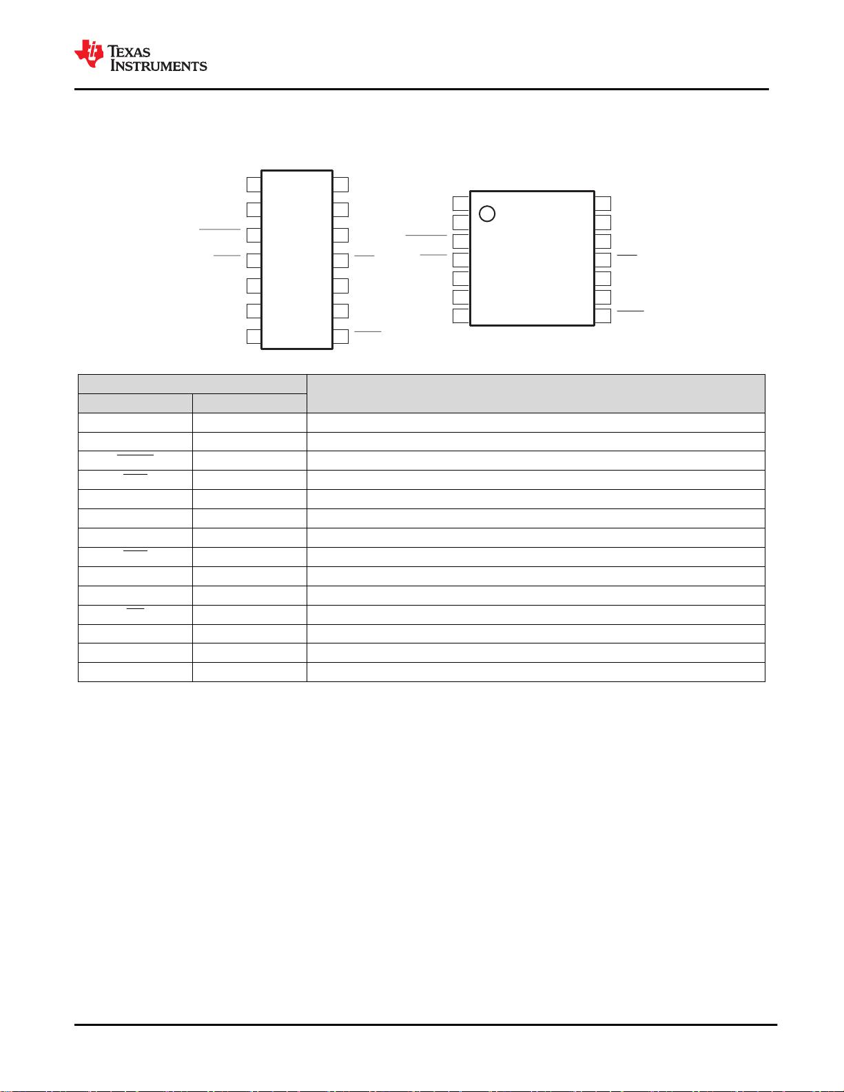
5 Pin Configuration and Functions...................................3
6 Specifications.................................................................. 4
6.1 Absolute Maximum Ratings........................................ 4
6.2 ESD Ratings............................................................... 4
6.3 Recommended Operating Conditions.........................4
6.4 Thermal Information....................................................5
6.5 Electrical Characteristics.............................................5
6.6 I
2
C Interface Timing Requirements.............................7
6.7 Switching Characteristics............................................8
6.8 Interrupt and Reset Timing Requirements.................. 8
7 Parameter Measurement Information............................ 9
8 Detailed Description...................................................... 11
8.1 Overview................................................................... 11
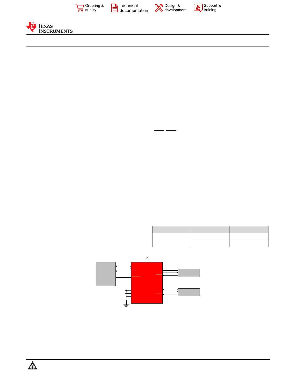
8.2 Functional Block Diagram......................................... 11
8.3 Feature Description...................................................12
8.4 Device Functional Modes..........................................12
8.5 Programming............................................................ 12
8.6 Control Register........................................................ 14
9 Application and Implementation.................................. 17
9.1 Application Information............................................. 17
9.2 Typical Application.................................................... 17
10 Power Supply Recommendations..............................20
10.1 Power-On Reset Requirements.............................. 20
11 Layout........................................................................... 22
11.1 Layout Guidelines................................................... 22
11.2 Layout Example...................................................... 22
12 Device and Documentation Support..........................23
12.1 Receiving Notification of Documentation Updates..23
12.2 Support Resources................................................. 23
12.3 Trademarks............................................................. 23
12.4 Electrostatic Discharge Caution..............................23
12.5 Glossary..................................................................23
13 Mechanical, Packaging, and Orderable
Information.................................................................... 23
4 Revision History
Changes from Revision A (April 2014) to Revision B (march 2021) Page
• 在
器件信息
表中添加了 SOIC 封装.....................................................................................................................1
• Deleted Package thermal impedance from the Absolute Maximum Ratings .....................................................4
• Moved the "Storage temperature range" to the Absolute Maximum Ratings .................................................... 4
• Changed the PW package values in the Thermal Information .......................................................................... 5
• Added D package values to the Thermal Information ........................................................................................5
• Changed the V
PORR
row in the Electrical Characteristics .................................................................................. 5
• Added V
PORF
row to the Electrical Characteristics ............................................................................................ 5
• Changed the I
CC
Low inputs and High inputs values in the Electrical Characteristics .......................................5
• Changed the C
i
SCL values in the Electrical Characteristics ............................................................................ 5
• Changed the R
on
(4.5 V to 5.5 V) TYP value From: 9 Ω To: 10 Ω in the Electrical Characteristics ................. 5
• Changed the R
on
(3 V to 3.6 V) TYP value From: 11 Ω To: 13 Ω in the Electrical Characteristics .................. 5
• Changed Pass-Gate Voltage (V
pass
) vs Supply Voltage (V
CC
) at Three Temperature Points ..........................19
• Changed the Power Supply Recommendations .............................................................................................. 20
Changes from Revision * (September 2007) to Revision A (April 2014) Page
• 删除了“订购信息”表........................................................................................................................................1
PCA9543A
ZHCSNJ4B – SEPTEMBER 2007 – REVISED MARCH 2021
www.ti.com.cn
2 Submit Document Feedback
Copyright © 2021 Texas Instruments Incorporated
Product Folder Links: PCA9543A
5 Pin Configuration and Functions
DPACKAGE
(TOP VIEW)
A0
A1
RESET
INT0
SD0
SC0
GND
V
CC
SDA
SCL
INT
SC1
SD1
INT1
1
2
3
4
5
6
7
14
13
12
11
10
9
8
PWPACKAGE
(TOP VIEW)
A0
A1
RESET
INT0
SD0
SC0
GND
1
2
3
4
5
6
7
V
CC
SDA
SCL
INT
SC1
SD1
INT1
14
13
12
11
10
9
8
表 5-1. Pin Functions
PIN
DESCRIPTION
NAME D, PW
A0 1 Address input 0. Connect directly to V
CC
or ground.
A1 2 Address input 1. Connect directly to V
CC
or ground.
RESET 3 Active-low reset input. Connect to V
CC
or V
DPUM
(1)
through a pull-up resistor, if not used.
INT0 4 Active-low interrupt input 0. Connect to V
DPU0
(1)
through a pull-up resistor.
SD0 5 Serial data 0. Connect to V
DPU0
(1)
through a pull-up resistor.
SC0 6 Serial clock 0. Connect to aV
DPU0
(1)
through a pull-up resistor.
GND 7 Ground
INT1 8 Active-low interrupt input 1. Connect to V
DPU1
(1)
through a pull-up resistor.
SD1 9 Serial data 1. Connect to V
DPU1
(1)
through a pull-up resistor.
SC1 10 Serial clock 1. Connect to V
DPU1
(1)
through a pull-up resistor.
INT 11 Active-low interrupt output. Connect to V
DPUM
(1)
through a pull-up resistor.
SCL 12 Serial clock line. Connect to V
DPUM
(1)
through a pull-up resistor.
SDA 13 Serial data line. Connect to V
DPUM
(1)
through a pull-up resistor.
VCC 14 Supply power
(1) V
DPUX
is the pull-up reference voltage for the associated data line. V
DPUM
is the master I
2
C reference voltage while V
DPU0
and V
DPU1
are the slave channel reference voltages.
www.ti.com.cn
PCA9543A
ZHCSNJ4B – SEPTEMBER 2007 – REVISED MARCH 2021
Copyright © 2021 Texas Instruments Incorporated
Submit Document Feedback
3
Product Folder Links: PCA9543A
6 Specifications
6.1 Absolute Maximum Ratings
over operating free-air temperature range (unless otherwise noted)
(1)
MIN MAX UNIT
V
CC
Supply voltage range
–0.5
7 V
V
I
Input voltage range
(2)
–0.5
7 V
I
I
Input current ±20 mA
I
O
Output current ±25 mA
Continuous current through V
CC
±100 mA
Continuous current through GND ±100 mA
P
tot
Total power dissipation 400 mW
T
A
Operating free-air temperature range
–40
85 °C
T
stg
Storage temperature range
–60
150 °C
(1) Stresses beyond those listed under “absolute maximum ratings” may cause permanent damage to the device. These are stress
ratings only, and functional operation of the device at these or any other conditions beyond those indicated under “recommended
operating conditions
” is not implied. Exposure to absolute-maximum-rated conditions for extended periods may affect device
reliability.
(2) The input negative-voltage and output voltage ratings may be exceeded if the input and output current ratings are observed.
6.2 ESD Ratings
MIN MAX UNIT
V
(ESD)
Electrostatic discharge
Human body model (HBM), per ANSI/ESDA/JEDEC JS-001, all
pins
(1)
0 2000
V
Charged device model (CDM), per JEDEC specification
JESD22-C101, all pins
(2)
0 1000
(1) JEDEC document JEP155 states that 500-V HBM allows safe manufacturing with a standard ESD control process.
(2) JEDEC document JEP157 states that 250-V CDM allows safe manufacturing with a standard ESD control process.
6.3 Recommended Operating Conditions
See
(1)
MIN MAX UNIT
V
CC
Supply voltage 2.3 5.5 V
V
IH
High-level input voltage
SCL, SDA 0.7 × V
CC
6
V
A1, A0, INT1, INT0, RESET
V
CC
= 2.3 V to 3.6 V 0.7 × V
CC
V
CC
+ 0.5
V
CC
= 3.6 V to 4.5 V 0.7 × V
CC
V
CC
+ 0.5
V
CC
= 4.5 V to 5.5 V 0.7 × V
CC
V
CC
+ 0.5
V
IL
Low-level input voltage
SCL, SDA
–0.5
0.3 × V
CC
V
A1, A0, INT1, INT0, RESET
–0.5
0.3 × V
CC
T
A
Operating free-air temperature
–40
85 °C
(1) All unused inputs of the device must be held at V
CC
or GND to ensure proper device operation. Refer to the TI application report,
Implications of Slow or Floating CMOS Inputs, literature number SCBA004.
PCA9543A
ZHCSNJ4B – SEPTEMBER 2007 – REVISED MARCH 2021
www.ti.com.cn
4 Submit Document Feedback
Copyright © 2021 Texas Instruments Incorporated
Product Folder Links: PCA9543A
6.4 Thermal Information
THERMAL METRIC
(1)
PCA9543A PCA9543A
UNIT
PW
(TSSOP)
D
(SOIC)
14 PINS 14 PINS
R
θJA
Junction-to-ambient thermal resistance 130.1 102.8
°C/W
R
θJCtop
Junction-to-case (top) thermal resistance 59.2 63.9
R
θJB
Junction-to-board thermal resistance 73.1 57.1
ψ
JT
Junction-to-top characterization parameter 11.7 26.7
ψ
JB
Junction-to-board characterization parameter 72.5 56.8
(1) For more information about traditional and new thermal metrics, see the IC Package Thermal Metrics application report, SPRA953.
6.5 Electrical Characteristics
over recommended operating free-air temperature range (unless otherwise noted)
(1)
PARAMETER TEST CONDITIONS V
CC
MIN TYP MAX UNIT
V
PORR
Power-on reset voltage,
V
CC
rising
No load: V
I
= V
CC
or GND
(2)
1.2 1.5 V
V
PORF
Power-on reset voltage,
V
CC
falling
No load: V
I
= V
CC
or GND
(2)
0.8 1 V
V
pass
Switch output voltage
V
SWin
= V
CC
,
I
SWout
= –100 μA
5 V 3.6
V
4.5 V to 5.5 V 2.6 4.5
3.3 V 1.9
3 V to 3.6 V 1.6 2.8
2.5 V 1.5
2.3 V to 2.7 V 1.1 2
I
OH
INT V
O
= V
CC
2.3 V to 5.5 V 100
μA
I
OL
SDA
V
OL
= 0.4 V
2.3 V to 5.5 V
3 7
mAV
OL
= 0.6 V 6 10
INT V
OL
= 0.4 V 3
I
I
SCL, SDA V
I
= V
CC
or GND 2.3 V to 5.5 V
–1
1
μA
SC1–SC0, SD1–SD0
V
I
= V
CC
or GND
2.3 V to 3.6 V
–1
1
4.5 V to 5.5 V
–1
100
A1, A0 V
I
= V
CC
or GND
2.3 V to 3.6 V
–1
1
4.5 V to 5.5 V
–1
50
INT1– INT0
V
I
= V
CC
or GND
2.3 V to 3.6 V
–1
1
4.5 V to 5.5 V
–1
50
RESET V
I
= V
CC
or GND
2.3 V to 3.6 V
–1
1
4.5 V to 5.5 V
–1
50
www.ti.com.cn
PCA9543A
ZHCSNJ4B – SEPTEMBER 2007 – REVISED MARCH 2021
Copyright © 2021 Texas Instruments Incorporated
Submit Document Feedback
5
Product Folder Links: PCA9543A
剩余31页未读,继续阅读
资源评论
不觉明了
- 粉丝: 3116
- 资源: 5348
上传资源 快速赚钱
- 我的内容管理 展开
- 我的资源 快来上传第一个资源
- 我的收益 登录查看自己的收益
- 我的积分 登录查看自己的积分
- 我的C币 登录后查看C币余额
- 我的收藏
- 我的下载
- 下载帮助
最新资源
- 电子万年历软件仿真(经过多次修改,保证正确性)
- Unity XR 手势射击控制脚本(适用于任何可手势识别的设备)
- 机械设计全自动电表(NB和IC卡表)控制和上壳装配线sw16可编辑非常好的设计图纸100%好用.zip
- 基于matlab的EAN-13条形码识别系统GUI界面.zip代码53
- matlab基于bp神经网络交通信号标志识别GUI界面13个标志.zip代码54
- 电子万年历答辩实物展示视频mp4格式
- 基于python实现的程序,包括哈希感知算法cvHash,图像切割cvsplit,固定目标检测cvRec(附文档ppt)等
- 计算0-10000之间所有偶数的和
- multiled.zip
- 基于php实现的哈希算法的人脸检索
资源上传下载、课程学习等过程中有任何疑问或建议,欢迎提出宝贵意见哦~我们会及时处理!
点击此处反馈
安全验证
文档复制为VIP权益,开通VIP直接复制
信息提交成功