没有合适的资源?快使用搜索试试~ 我知道了~
TI-PCA9544A.pdf
需积分: 10 0 下载量 153 浏览量
2023-02-08
20:48:06
上传
评论 4
收藏 2.72MB PDF 举报
温馨提示
试读
39页
I2C开关
资源推荐
资源详情
资源评论
具有中断逻辑的 PCA9544A 低电压 4 通道 I
2
C 和 SMBus 多路复用器
1 特性
• 4 选 1 双向转换开关
• 与 I
2
C 总线和 SMBus 兼容
• 四个低电平有效中断输入
• 低电平有效中断输出
• 三个地址引脚,I
2
C 总线上最多支持八个器件
• 通过 I
2
C 总线选择通道
• 加电时所有开关通道取消选定
• 低 R
ON
开关
• 支持在 1.8V、2.5V、3.3V 和 5V 总线间进行电压电
平转换
• 加电时无干扰
• 支持热插入
• 低待机电流
• 工作电源电压范围为 2.3V 至 5.5V
• 5.5V 耐压输入
• 0 至 400kHz 时钟频率
• 闩锁性能超过 100mA,符合 JESD 78 规范
• ESD 保护性能超出 JESD 22 标准
– 2000V 人体放电模型 (A114-A)
– 200V 机器模型 (A115-A)
– 1000V 充电器件模型 (C101)
2 应用
• 服务器
• 路由器(电信交换设备)
• 工厂自动化
• 具有 I
2
C 从地址冲突的产品(例如,多个完全一样
的温度传感器)
3 说明
PCA9544A 是一款由 I2C 总线控制的 4 通道双向转换
多路复用器。SCL/SDA 上行对扩展到四个下行对,或
者通道。根据可编程控制寄存器的内容,每次可选择任
一 SCL/SDA 对。提供四个中断输入 (INT3-INT0),每
个中断输入针对一个下行对。一个中断输出 (INT) 是四
个中断输入的与运算结果。
上电复位功能使寄存器处于缺省状态,并初始化 I2C
状态机,无需选择任何通道。
由于开关上有导通栅极,因此 VCC 引脚可用于限制将
由 PCA9544A 传递的最大电压。这允许在每个对上使
用不同的总线电压,以便 1.8V,2.5V 或 3.3V 部件可
以在没有任何额外保护的情况下与 5V 部件通信。对于
每个通道,外部上拉电阻器将总线电压上拉至所需的电
压水平。所有 I/O 引脚均可承受 5V 电压。
器件信息
器件型号
封装
(1)
封装尺寸(标称值)
PCA9544A
TVSOP (DGV) (20) 5.00mm x 4.40mm
SOIC (DW) (20) 12.8mm x 7.50mm
TSSOP (PW) (20) 6.50mm × 4.40mm
VQFN (RGY) (20) 4.50mm x 3.50mm
(1) 如需了解所有可用封装,请参阅数据表末尾的可订购产品附
录。
PCA9544A
Slaves A , A ...A0 1 N
Slaves B , B ...B0 1 N
I2C or SMBus
Master
(e.g. µProcessor)
SDA
SCL
INT
SD0
SC0
INT0
Channel 0
Channel 1
SD1
SC1
INT1
V
CC
A0
A1
GND
A2
Slaves B , B ...B0 1 N
Channel 2
SD2
SC2
INT2
Slaves B , B ...B0 1 N
Channel 3
SD3
SC3
INT3
简化版应用示意图
PCA9544A
ZHCSK60G – OCTOBER 2005 – REVISED MARCH 2021
本文档旨在为方便起见,提供有关 TI 产品中文版本的信息,以确认产品的概要。有关适用的官方英文版本的最新信息,请访问
www.ti.com,其内容始终优先。TI 不保证翻译的准确性和有效性。在实际设计之前,请务必参考最新版本的英文版本。
English Data Sheet: SCPS146
Table of Contents
1 特性................................................................................... 1
2 应用................................................................................... 1
3 说明................................................................................... 1
4 Revision History.............................................................. 2
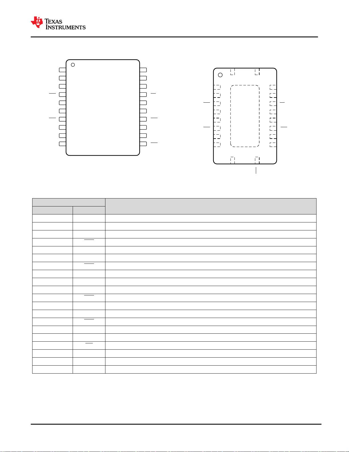
5 Pin Configuration and Functions...................................3
6 Specifications.................................................................. 4
6.1 Absolute Maximum Ratings........................................ 4
6.2 ESD Ratings............................................................... 4
6.3 Recommended Operating Conditions.........................4
6.4 Thermal Information....................................................4
6.5 Electrical Characteristics.............................................6
6.6 I
2
C Interface Timing Requirements.............................8
6.7 Switching Characteristics............................................8
6.8 Interrupt Timing Requirements....................................8
7 Parameter Measurement Information............................ 9
8 Detailed Description...................................................... 11
8.1 Overview................................................................... 11
8.2 Functional Block Diagram......................................... 12
8.3 Feature Description...................................................13
8.4 Device Functional Modes..........................................13
8.5 Programming............................................................ 13
8.6 Register Map.............................................................15
9 Application Information Disclaimer............................. 18
9.1 Application Information............................................. 18
9.2 Typical Application.................................................... 18
10 Power Supply Recommendations..............................22
10.1 Power-On Reset Requirements.............................. 22
11 Layout........................................................................... 24
11.1 Layout Guidelines................................................... 24
11.2 Layout Example...................................................... 24
12 Device and Documentation Support..........................25
12.1 Receiving Notification of Documentation Updates..25
12.2 支持资源..................................................................25
12.3 Trademarks.............................................................25
12.4 静电放电警告.......................................................... 25
12.5 术语表..................................................................... 25
13 Mechanical, Packaging, and Orderable
Information.................................................................... 25
4 Revision History
Changes from Revision F (August 2019) to Revision G (March 2021) Page
• Changed the PW packgae values in the Thermal Information table...................................................................4
• Added the RGY package values in the Thermal Information table.....................................................................4
• Changed the V
PORR
row in the Electrical Characteristics .................................................................................. 6
• Added V
PORF
row to the Electrical Characteristics ............................................................................................ 6
• Changed the I
CC
Low inputs and High inputs values in the Electrical Characteristics .......................................6
• Changed the ΔI
CC
(INT3–INT0) MAX values From: 15 µA To: 20 µA in the Electrical Characteristics ...........6
• Changed the Application Curves ..................................................................................................................... 21
• Changed the Power Supply Recommendations .............................................................................................. 22
Changes from Revision E (June 2014) to Revision F (August 2019) Page
• 将文本从“PCA9544A 是一款四路双向转换开关”更改为“PCA9544A 是一款 4 通道双向转换多路复用器”
(在说明 中)。..................................................................................................................................................1
• 更改了
器件信息
表.............................................................................................................................................. 1
• Deleted the RGW, GQN, and ZQN packages from the Pin Configuration and Functions section......................3
• Moved T
stg
to the Absolute Maximum Ratings .................................................................................................. 4
• Changed the Handling Ratings table to ESD Ratings table................................................................................4
• Added the Thermal Information table................................................................................................................. 4
• Changed the first paragraph of the Overview section.......................................................................................11
• Changed text From: "bidirectional translating switch" To: "bidirectional translating multiplexer"...................... 13
• Changed text from: "One or several SCn/SDn downstream pairs or channels, are selected" To: "Only one
SCn/SDn downstream pair, or channel, can be selected" in the Control Register Definition section............... 16
• Deleted sentence: "If multiple switches will be enabled.." from the second paragraph of the Application
Information section........................................................................................................................................... 18
Changes from Revision D (February 2008) to Revision E (June 2014) Page
PCA9544A
ZHCSK60G – OCTOBER 2005 – REVISED MARCH 2021
www.ti.com.cn
2 Submit Document Feedback
Copyright © 2021 Texas Instruments Incorporated
Product Folder Links: PCA9544A
5 Pin Configuration and Functions
1A0 20
V
CC
2A1 19 SDA
3A2 18 SCL
4INT0 17 INT
5SD0 16 SC3
6SC0 15 SD3
7INT1 14 INT3
8SD1 13 SC2
9SC1 12 SD2
10GND 11 INT2
No t to scale
图 5-1. DGV, DW, or PW Package, TVSOP, SOIC,
TSSOP (20 Pins), Top View
Th ermal
Pad
2A1
3A2
4INT0
5SD0
6SC0
7INT1
8SD1
9SC1
10GND
11INT2
12 SD2
13 SC2
14 INT3
15 SD3
16 SC3
17 INT
18 SCL
19 SDA
20
V
CC
1 A0
No t to scale
图 5-2. RGY Package, VQFN (20 Pins), Top View
表 5-1. Pin Functions
PIN
FUNCTION
NO. NAME
1 A0 Address input 0. Connect directly to V
CC
or ground.
2 A1 Address input 1. Connect directly to V
CC
or ground.
3 A2 Address input 2. Connect directly to V
CC
or ground.
4 INT0 Active-low interrupt input 0. Connect to V
DPU0
(1)
through a pull-up resistor.
5 SD0 Serial data 0. Connect to V
DPU0
(1)
through a pull-up resistor.
6 SC0 Serial clock 0. Connect to V
DPU0
(1)
through a pull-up resistor.
7 INT1 Active-low interrupt input 1. Connect to V
DPU1
(1)
through a pull-up resistor.
8 SD1 Serial data 1. Connect to V
DPU1
(1)
through a pull-up resistor.
9 SC1 Serial clock 1. Connect to V
DPU1
(1)
through a pull-up resistor.
10 GND Ground
11 INT2 Active-low interrupt input 2. Connect to V
DPU2
(1)
through a pull-up resistor.
12 SD2 Serial data 2. Connect to V
DPU2
(1)
through a pull-up resistor.
13 SC2 Serial clock 2. Connect to V
DPU2
(1)
through a pull-up resistor.
14 INT3 Active-low interrupt input 3. Connect to V
DPU3
(1)
through a pull-up resistor.
15 SD3 Serial data 3. Connect to V
DPU3
(1)
through a pull-up resistor.
16 SC3 Serial clock 3. Connect to V
DPU3
(1)
through a pull-up resistor.
17 INT Active-low interrupt output. Connect to V
DPUM
(1)
through a pull-up resistor.
18 SCL Serial clock line. Connect to V
DPUM
(1)
through a pull-up resistor.
19 SDA Serial data line. Connect to V
DPUM
(1)
through a pull-up resistor.
20 VCC Supply power
(1) V
DPUX
is the pull-up reference voltage for the associated data line. V
DPUM
is the master I
2
C reference voltage while V
DPU0
-V
DPU3
are
the slave channel reference voltages.
www.ti.com.cn
PCA9544A
ZHCSK60G – OCTOBER 2005 – REVISED MARCH 2021
Copyright © 2021 Texas Instruments Incorporated
Submit Document Feedback
3
Product Folder Links: PCA9544A
6 Specifications
6.1 Absolute Maximum Ratings
over operating free-air temperature range (unless otherwise noted)
(1)
MIN MAX UNIT
V
CC
Supply voltage range
–0.5
7 V
V
I
Input voltage range
(2)
–0.5
7 V
I
I
Input current ±20 mA
I
O
Output current ±25 mA
Continuous current through V
CC
±100 mA
Continuous current through GND ±100 mA
P
tot
Total power dissipation 400 mW
T
A
Operating free-air temperature range
–40
85 °C
T
stg
Storage temperature range
–60
150
°C
(1) Stresses beyond those listed under "absolute maximum ratings" may cause permanent damage to the device. These are stress ratings
only, and functional operation of the device at these or any other conditions beyond those indicated under "recommended operating
conditions" is not implied. Exposure to absolute-maximum-rated conditions for extended periods may affect device reliability.
(2) The input negative-voltage and output voltage ratings may be exceeded if the input and output current ratings are observed.
6.2 ESD Ratings
MIN MAX UNIT
V
(ESD)
Electrostatic discharge
Human body model (HBM), per ANSI/ESDA/JEDEC JS-001, all pins
(1)
0 2000
V
Charged device model (CDM), per JEDEC specification JESD22-C101, all
pins
(2)
0 1000
(1) JEDEC document JEP155 states that 500-V HBM allows safe manufacturing with a standard ESD control process.
(2) JEDEC document JEP157 states that 250-V CDM allows safe manufacturing with a standard ESD control process.
6.3 Recommended Operating Conditions
See
(1)
MIN MAX UNIT
V
CC
Supply voltage 2.3 5.5 V
V
IH
High-level input voltage
SCL, SDA 0.7 × V
CC
6
V
A2–A0, INT3– INT0
0.7 × V
CC
V
CC
+ 0.5
V
IL
Low-level input voltage
SCL, SDA
–0.5
0.3 × V
CC
V
A2–A0, INT3– INT0 –0.5
0.3 × V
CC
T
A
Operating free-air temperature
–40
85 °C
(1) All unused inputs of the device must be held at V
CC
or GND to ensure proper device operation. Refer to the TI application report,
Implications of Slow or Floating CMOS Inputs.
6.4 Thermal Information
THERMAL METRIC
(1)
PCA9544A
UNITDGV DW PW RGY
20 PINS 20 PINS 20 PINS 20 PINS
R
θJA
Junction-to-ambient thermal resistance 92 58 118.2 62.7 °C/W
R
θJC(top)
Junction-to-case (top) thermal resistance 43.9 41.9 62.7 60.5 °C/W
R
θJB
Junction-to-board thermal resistance 64.5 40.3 69.3 39.5 °C/W
ψ
JT
Junction-to-top characterization parameter 4.2 18.1 7.7 7.2 °C/W
ψ
JB
Junction-to-board characterization parameter 63.6 40 68.8 39.8 °C/W
PCA9544A
ZHCSK60G – OCTOBER 2005 – REVISED MARCH 2021
www.ti.com.cn
4 Submit Document Feedback
Copyright © 2021 Texas Instruments Incorporated
Product Folder Links: PCA9544A
6.4 Thermal Information (continued)
THERMAL METRIC
(1)
PCA9544A
UNITDGV DW PW RGY
20 PINS 20 PINS 20 PINS 20 PINS
R
θJC(bot)
Junction-to-case (bottom) thermal resistance n/a n/a n/a 26.6 °C/W
(1) For more information about traditional and new thermal metrics, see the Semiconductor and IC package thermal metrics application
report.
www.ti.com.cn
PCA9544A
ZHCSK60G – OCTOBER 2005 – REVISED MARCH 2021
Copyright © 2021 Texas Instruments Incorporated
Submit Document Feedback
5
Product Folder Links: PCA9544A
剩余38页未读,继续阅读
资源评论
不觉明了
- 粉丝: 3117
- 资源: 5348
上传资源 快速赚钱
- 我的内容管理 展开
- 我的资源 快来上传第一个资源
- 我的收益 登录查看自己的收益
- 我的积分 登录查看自己的积分
- 我的C币 登录后查看C币余额
- 我的收藏
- 我的下载
- 下载帮助
安全验证
文档复制为VIP权益,开通VIP直接复制
信息提交成功