TI-TSU5611.pdf
需积分: 5 181 浏览量
2022-12-03
09:43:33
上传
评论 4
收藏 783KB PDF 举报


A B C D
E
1
2
3
4
TSU5611
www.ti.com.cn
ZHCS405 –AUGUST 2011
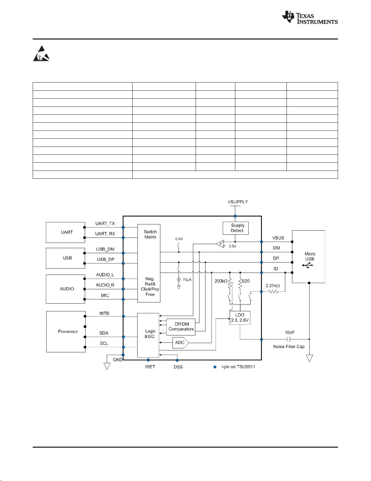
DP3T开关是具有阻抗检测功能的微型USB开关
可以支持USB, UART, 音频, 和充电设备检测
查询样品
: TSU5611
1
特性
YZP 封装
• 兼容附件
顶视图
– USB 数据线缆
– UART 线缆
– 充电设备(专用充电设备或者主机/充电设备)
– 有麦克风的立体声耳机
• 用于VREF和麦克偏置电压的集成低压线性稳压
器(LDOs)
• USB 和UART路径支持 USB 2.0高速接口
• 音频通道提供负轨道支持和
• 支持工厂测试模式
• 1.8-V 兼容 I
2
C 接口
• 控制输入符合 1.8 V 逻辑要求
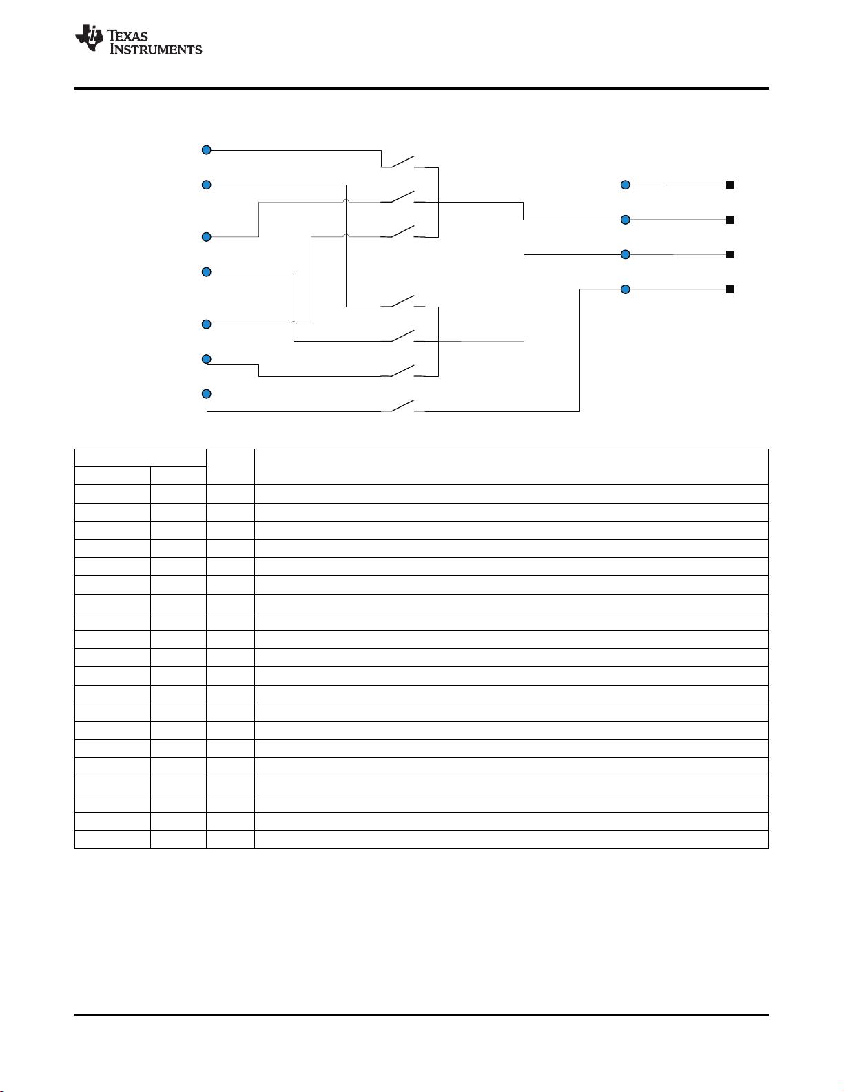
针脚指定
– 1500-V 人体模型
A B C D E
(A114-B, Class II)
4 MIC ISET UART_TX USB_DM USB_DP
– 1000 V 充电器件模型(C101)
3 R2.2K INT UART_RX ID DP
2 SDA SCL DSS GND 数据手册
应用
1 CLDO V
供电
AUDIO_R AUDIO_L V
BUS
• 手机与智能电话
• 平板 PC
• 数码相机与摄像机
• 全球卫星定位(GPS)导航系统
• 具有USB/UART的微型USB接口
说明
TSU5611被设计成能够与手机UART,USB和通过微型USB连接器与外部设备连接的音频芯片进行连接。 这个开关
特有阻抗检测功能用以识别通过微型USB端口的DP和DM连接的多种配件。 当一个配件插入到微型USB端口时, 这
个开关使用侦测机制以识别这个配件(详细信息请参考State Machine期刊). 然后它将切换到合适的频道—数据, 音
频, 或者UART。
TSU5611有一个 I2C接口用于与手机基带或者应用设备处理器进行通信。 当微型USB接口侦测到任何插入设时,
一个中断会产生。 当设备拔出时,产生另外一个中断。
ORDERING INFORMATION
(1)
T
A
PACKAGE
(2)
ORDERABLE PART NUMBER TOP-SIDE MARKING
–40°C to 85°C WSCP–YZP (0.5-mm pitch) Tape and Reel TSU5611YZPR A7
(1) For the most current package and ordering information, see the Package Option Addendum at the end of this document, or see the TI
Web site at www.ti.com.
(2) Package drawings, thermal data, and symbolization are available at www.ti.com/packaging.
1
Please be aware that an important notice concerning availability, standard warranty, and use in critical applications of Texas
Instruments semiconductor products and disclaimers thereto appears at the end of this data sheet.
PRODUCTION DATA information is current as of publication date.
Copyright © 2011, Texas Instruments Incorporated
Products conform to specifications per the terms of the Texas
Instruments standard warranty. Production processing does not English Data Sheet: SCDS326
necessarily include testing of all parameters.
剩余27页未读,继续阅读
资源评论


