TI-TSU8111.pdf
需积分: 5 147 浏览量
2022-12-01
23:36:23
上传
评论 4
收藏 1.31MB PDF 举报

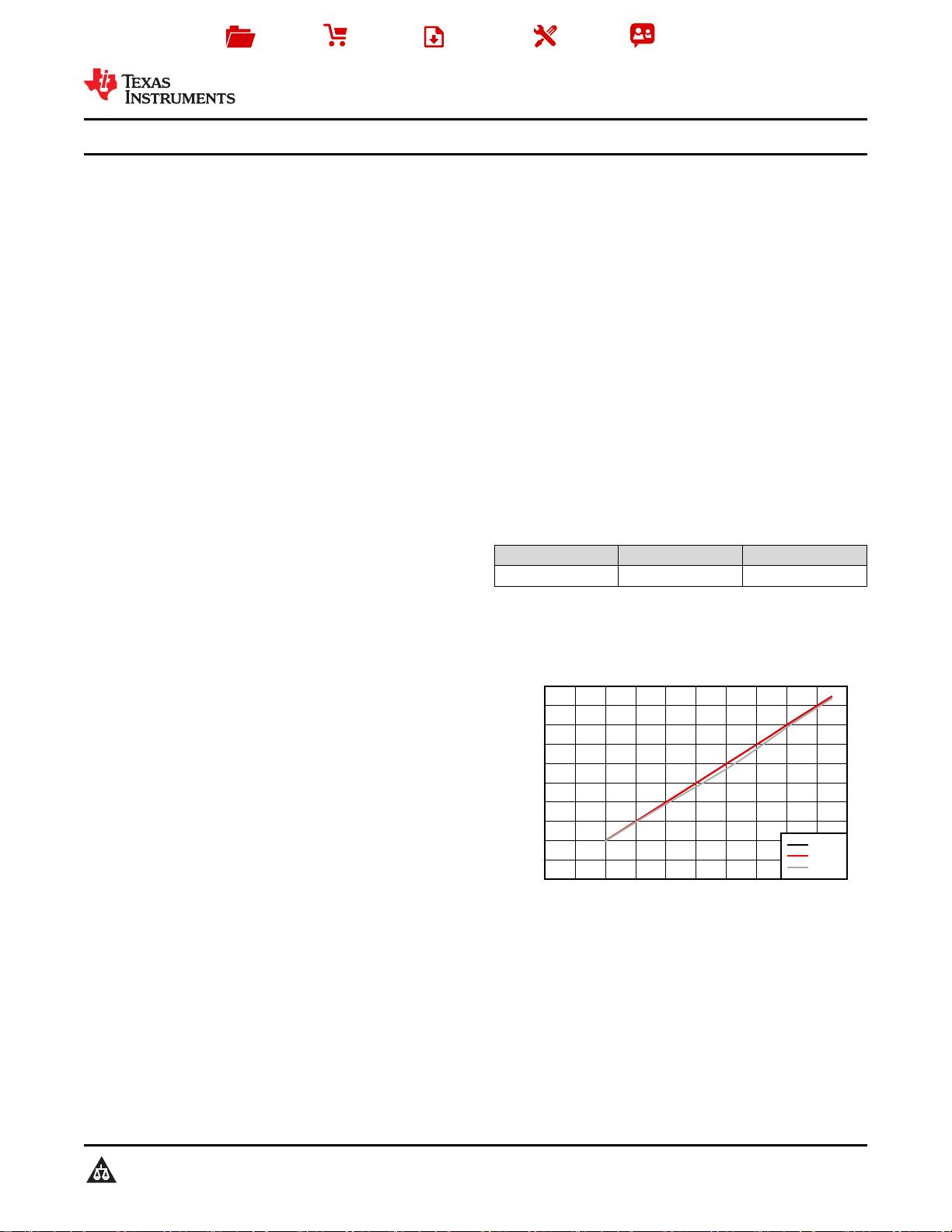
ISET Curent Setting in Register 22h (mA)
Actual LDO Output Current (mA)
0 100 200 300 400 500 600 700 800 900 1000
0
100
200
300
400
500
600
700
800
900
1000
D001
-40°C
25°C
85°C
Product
Folder
Sample &
Buy
Technical
Documents
Tools &
Software
Support &
Community
TSU8111
ZHCSAE4A –SEPTEMBER 2012–REVISED AUGUST 2014
TSU8111 具具有有单单节节充充电电器器的的双双路路 SP2T USB 2.0 高高速速开开关关
1 特特性性 2 应应用用范范围围
1
• 双单刀双掷 (SP2T) USB 2.0 高速开关
• 移动电话
• 上网本/笔记本电脑
– UART 路径支持 UART 或 USB 2.0 高速信号
• 台式机
• 集成单节充电器
• 便携式手持设备
– 集成低压降线性稳压器 (LDO)
– 充电电压稳压精度 1%
3 说说明明
– 充电电流精度 8%
TSU8111是一款具有集成线性充电器的双 SP2T 微型
– 针对壁式适配器的高达 950mA 的可编程充电电
USB 开关。 由于此器件集成有充电器,因此无需配备
流限制
外部充电器 IC,从而节省了成本与电路板空间。 该器
• 充电器检测符合 USB 电池充电规范 v1.1 (BCv1.1)
件可通过 USB 端口或专用充电器供电运行,并支持高
– VBUS 检测
达 950mA 的充电电流。 连接该器件后,将通过 VBAT
– 数据接触侦测
或 VBUS 为其供电。 TSU8111 可检测与 BCv1.1 标
– 主和副侦测
准兼容的充电器以及使用 ID 电阻的附件。 USB 开关
– 支持 USB 充电器(DCP、CDP、SDP)
矩阵既可以通过自动检测来控制,也可以通过 I
2
C 手动
• 可在 ID 引脚上进行 5 位附件检测
进行控制。
– 按附件类型自动切换
• I
2
C 接口
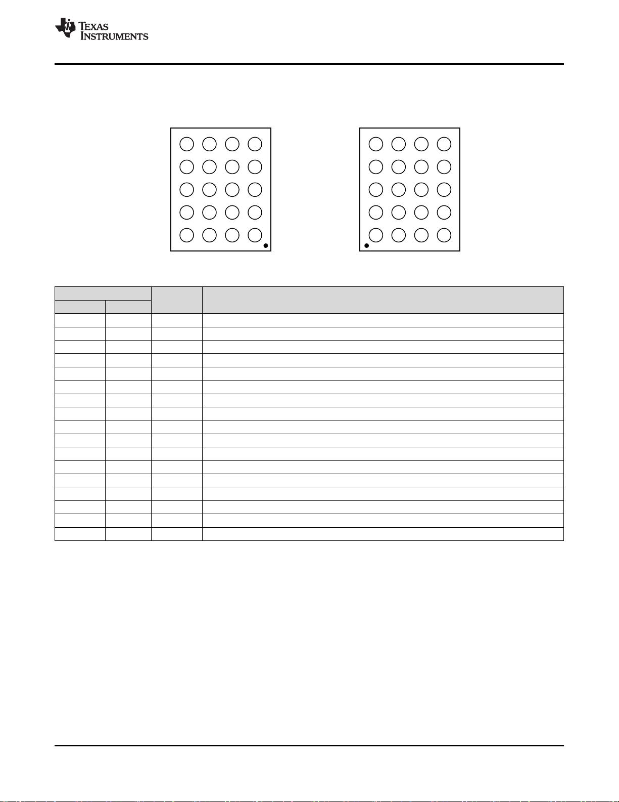
器器件件信信息息
(1)
– 手动切换功能
部部件件号号 封封装装 封封装装尺尺寸寸((标标称称值值))
– 连接和断开时产生中断
TSU8111 DSBGA (20) 2.14mm x 1.76mm
– 支持制造中使用的控制信号(JIG,BOOT)
(1) 如需了解所有可用封装,请参见数据表末尾的可订购产品附
录。
• 具有过压保护功能的 VBUS 引脚的容差为 28V
• 针对输出电流控制的热调节和热关断保护
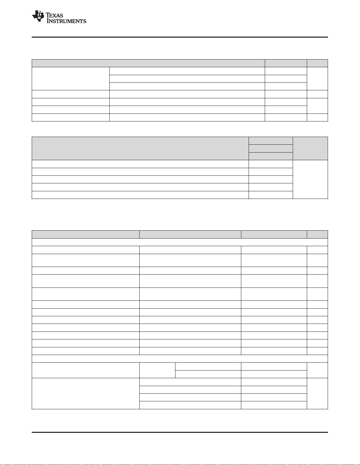
整整个个器器件件温温度度范范围围内内的的实实际际快快速速充充电电电电流流与与寄寄存存器器电电阻阻
• JESD 22 ESD 性能
设设置置间间的的关关系系
– 12kV 人体模型
(VBUS/DP_CON/DM_CON/ID_CON)
– 2kV 人体模型(所有其他引脚)
• IEC ESD 性能
– ±4kV 接触放电 (IEC 61000-4-
2)(VBUS/DP_CON/DM_CON/ID_CON 接地
(GND))
• 浪涌保护(VBUS/DP_CON/DM_CON/ID_CON 接
地)
– 无需使用外部元件即可保护 USB 连接器引脚
1
PRODUCTION DATA information is current as of publication date. Products conform to specifications per the terms of the Texas
Instruments standard warranty. Production processing does not necessarily include testing of all parameters.
English Data Sheet: SCDS335
剩余34页未读,继续阅读
资源评论


