TI-TSU6111A.pdf
需积分: 9 46 浏览量
2022-12-01
23:34:13
上传
评论 4
收藏 1.46MB PDF 举报

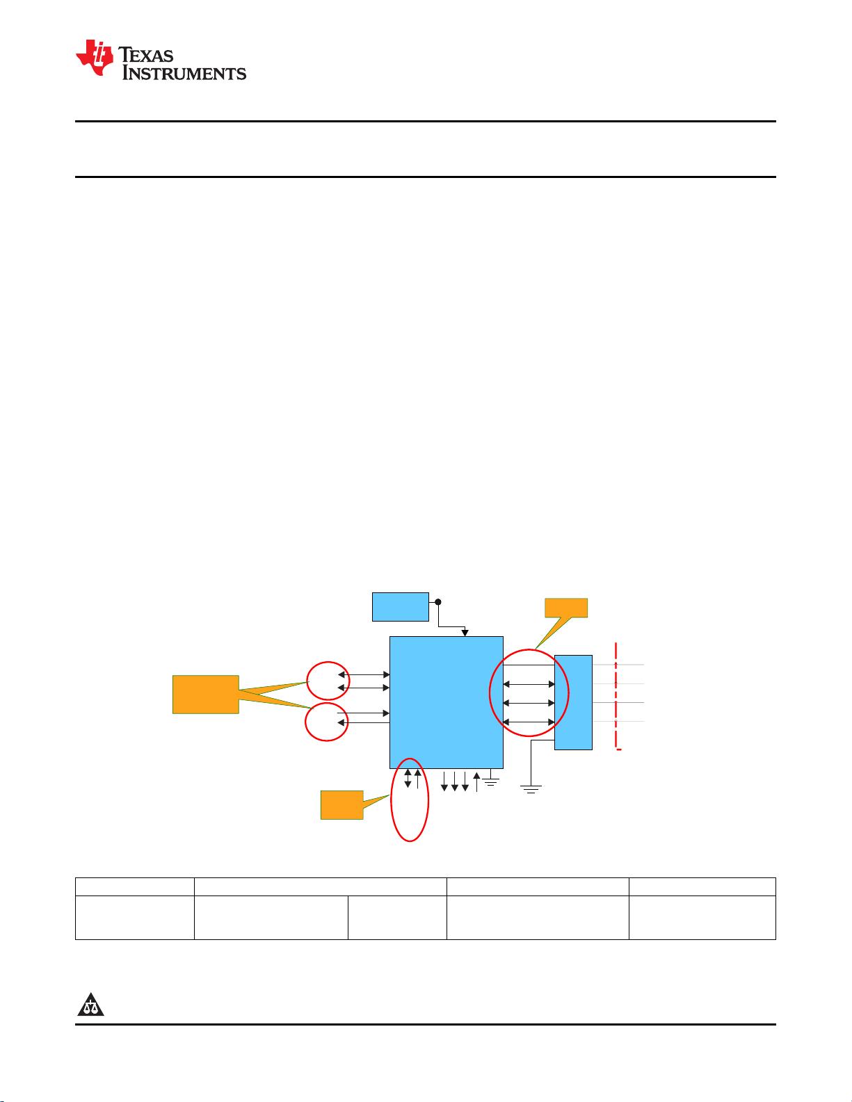
USB CONNECTOR
BATTERY
VBAT
RxD
TxD
DP_HT
DM_HT
MICMICMICMIC
ID_CON
DP_CON
VBUS
DM_CON
TSU6111
I2C_SDA
INTB
BOOT
JIG
I2C_SCL
VDDIO
USB
UART
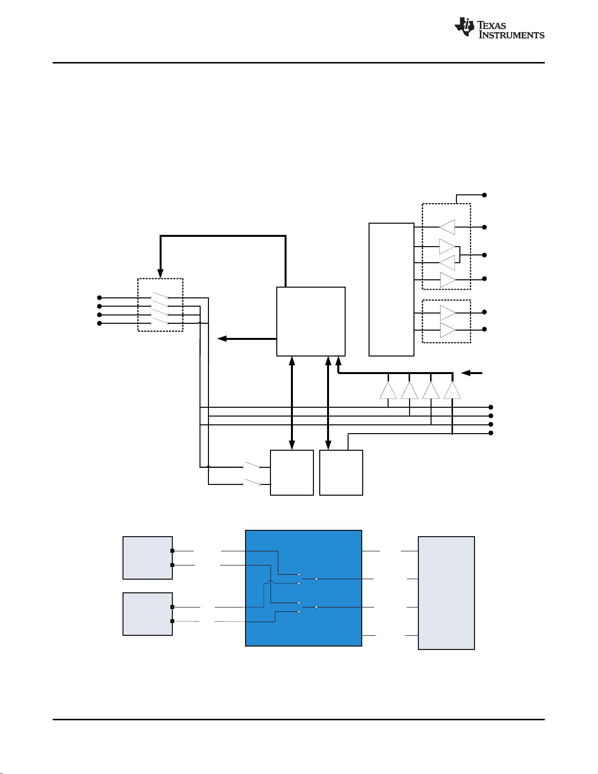
inside
outside
VBUS
ID_CON
DP_CON
DM_CON
IEC ESD
I2C
Control
USB2.0 High
Speed
USB2.0 High
Speed
TSU6111A
www.ti.com.cn
ZHCS744A –FEBRUARY 2012–REVISED AUGUST 2012
USB 端端口口单单刀刀双双掷掷 (SP2T) 开开关关支支持持 USB 和和通通用用异异步步接接收收发发器器 (UART)
查查询询样样品品: TSU6111A
1
特特性性
• 最最大大电电压压
– 额额定定 28V VBUS
• 开开关关矩矩阵阵
• 静静电电放放电电 (ESD) 性性能能测测试试符符合合 JESD 22 标标准准
– USB
– 5000V 人人体体模模型型
– UART 支支持持高高速速 USB 2.0
((A114-B,,II 类类))
• 充充电电设设备备侦侦测测
– 1000-V 充充电电器器件件模模型型 (C101)
– 与与 USB BCDv1.1 兼兼容容
• IEC ESD 性性能能
– VBUS 检检测测
– 针针对对 VBUS/DP_CON/DM_CON/ID_CON 接接地地
– 数数据据接接触触检检测测
(GND) 的的±8kV 接接触触放放电电 (IEC 61000-4-2)
– 一一级级和和二二级级检检测测
• VBUS/DP_CON/DM_CON 上上的的冲冲击击保保护护
• 兼兼容容附附件件
– 无无需需外外部部组组件件的的 USB 连连接接器器引引脚脚
– USB 充充电电器器 ((专专用用充充电电端端口口 (DCP),,充充电电下下行行
端端口口 (CDP)))
应应用用范范围围
– 厂厂家家电电缆缆
• 手手机机与与智智能能电电话话
• 附附加加特特性性
• 平平板板电电脑脑
– 与与主主机机处处理理器器的的 I
2
C 接接口口
• 数数码码相相机机与与摄摄像像机机
– 由由自自动动侦侦测测或或者者手手动动控控制制的的开开关关
• 全全球球卫卫星星定定位位 (GPS) 导导航航系系统统
– 为为插插/拔拔生生成成的的中中断断
• 具具有有 USB/UART 的的微微型型 USB 接接口口
– 支支持持制制造造中中使使用用的的控控制制信信号号 (JIG,,BOOT)
典典型型应应用用图图
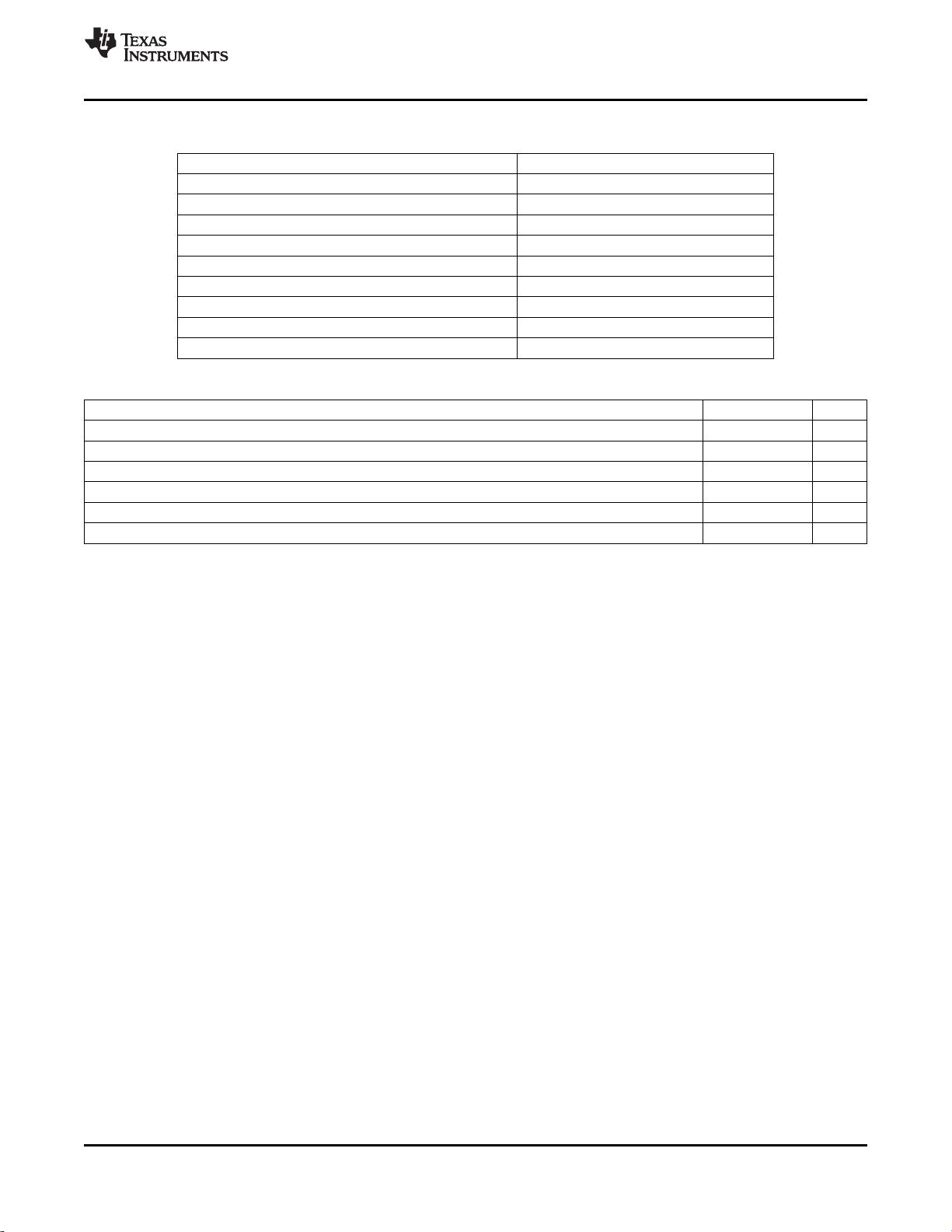
订订购购信信息息
(1)
T
A
封封装装
(2)
可可订订购购部部件件号号 正正面面标标记记
–40°C 至 85°C 超薄四方扁平无引线封装 卷带封装 TSU6111ARSVR ZTN
(uQFN) 0.4-mm 引脚中心距 -
RSV
(1) 要获得最新的封装和订购信息,请见本文档末尾的封装选项附录,或者浏览 TI 网站 www.ti.com。
(2) 封装图样、热数据和符号可登录 www.ti.com/packaging 获取。
1
Please be aware that an important notice concerning availability, standard warranty, and use in critical applications of
Texas Instruments semiconductor products and disclaimers thereto appears at the end of this data sheet.
PRODUCTION DATA information is current as of publication date.
版权 © 2012, Texas Instruments Incorporated
Products conform to specifications per the terms of the Texas
Instruments standard warranty. Production processing does not English Data Sheet: SCDS331
necessarily include testing of all parameters.
剩余33页未读,继续阅读


评论0
最新资源