TI-SN74LV4046A.pdf
需积分: 9 25 浏览量
2022-11-30
23:32:32
上传
评论 4
收藏 1.14MB PDF 举报


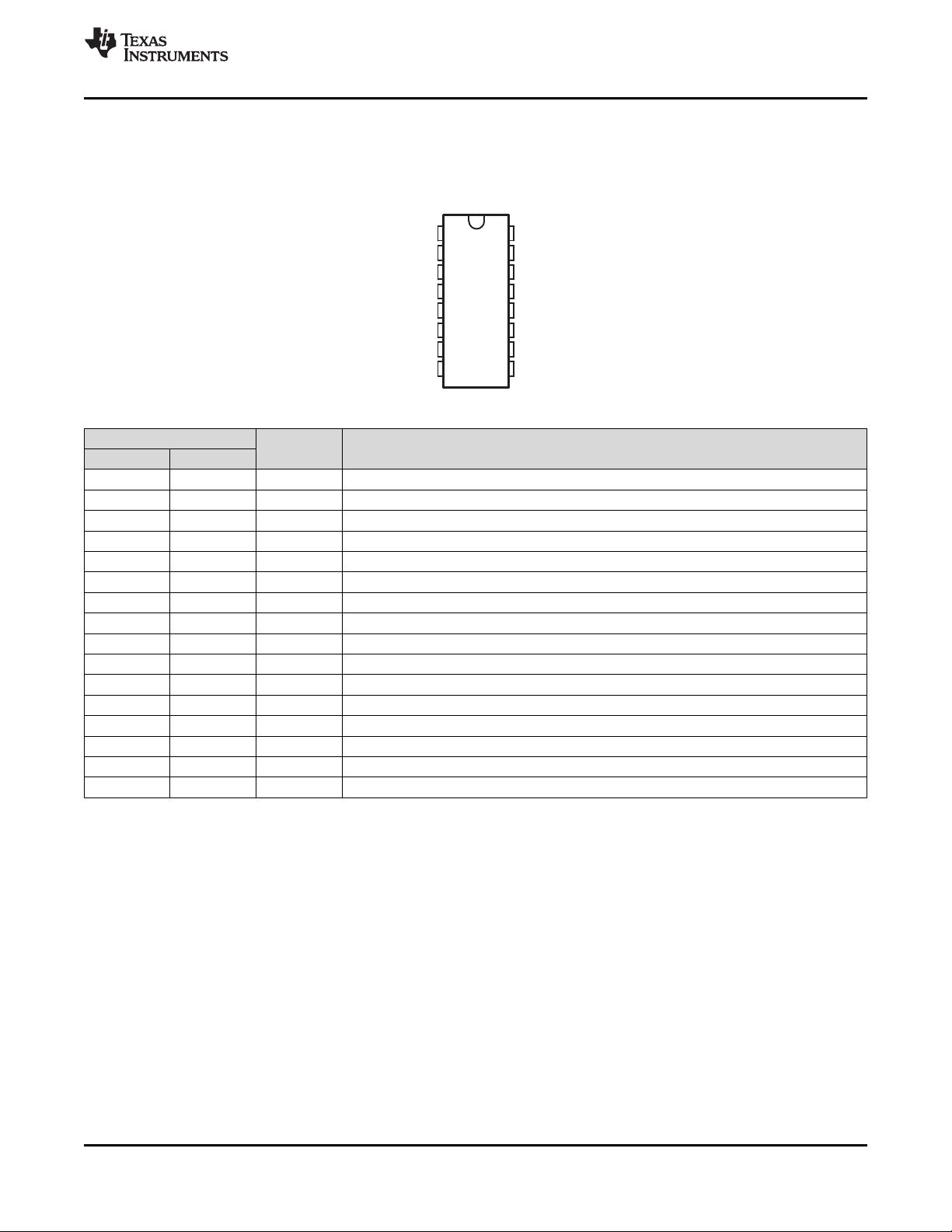
Voltage
Controlled
Oscillator
Phase
Comparator
1
Phase
Comparator
2
Phase
Comparator
3
3COMP
IN
SIG
IN
14
2 PC1
OUT
PCP
OUT
1
5INH
VCO
OUT
4
7C1
B
C1
A
6
9VCO
IN
GND
8
11R
1
DEM
OUT
10
13 PC2
OUT
R
2
12
15 PC3
OUT
V
CC
16
Product
Folder
Sample &
Buy
Technical
Documents
Tools &
Software
Support &
Community
An IMPORTANT NOTICE at the end of this data sheet addresses availability, warranty, changes, use in safety-critical applications,
intellectual property matters and other important disclaimers. PRODUCTION DATA.
SN74LV4046A
SCES656E –FEBRUARY 2006–REVISED NOVEMBER 2016
SN74LV4046A High-Speed CMOS Logic Phase-Locked Loop With VCO
1
1 Features
1
• ESD Protection Exceeds JESD 22
– 2000-V Human Body Model (A114-A)
– 1000-V Charged-Device Model (C101)
• Choice of Three Phase Comparators
– Exclusive OR
– Edge-Triggered J-K Flip-Flop
– Edge-Triggered RS Flip-Flop
• Excellent VCO Frequency Linearity
• VCO-Inhibit Control for ON/OFF Keying and for
Low Standby Power Consumption
• Optimized Power-Supply Voltage Range From
3 V to 5.5 V
• Wide Operating Temperature Range From
–40°C to +125°C
• Latch-Up Performance Exceeds 250 mA Per
JESD 17
2 Applications
• Telecommunications
• Signal Generators
• Digital Phase-Locked Loop
3 Description
The SN74LV4046A is a high-speed silicon-gate
CMOS device that is pin compatible with the
CD4046B and the CD74HC4046. The device is
specified in compliance with JEDEC Std 7.
The SN74LV4046A is a phase-locked loop (PLL)
circuit that contains a linear voltage-controlled
oscillator (VCO) and three different phase
comparators (PC1, PC2, and PC3). A signal input
and a comparator input are common to each
comparator.
The signal input can be directly coupled to large
voltage signals, or indirectly coupled (with a series
capacitor) to small voltage signals. A self-bias input
circuit keeps small voltage signals within the linear
region of the input amplifiers. With a passive low-
pass filter, the SN74LV4046A forms a second-order
loop PLL. The excellent VCO linearity is achieved by
the use of linear operational amplifier techniques.
Various applications include telecommunications,
digital phase-locked loop and signal generators.
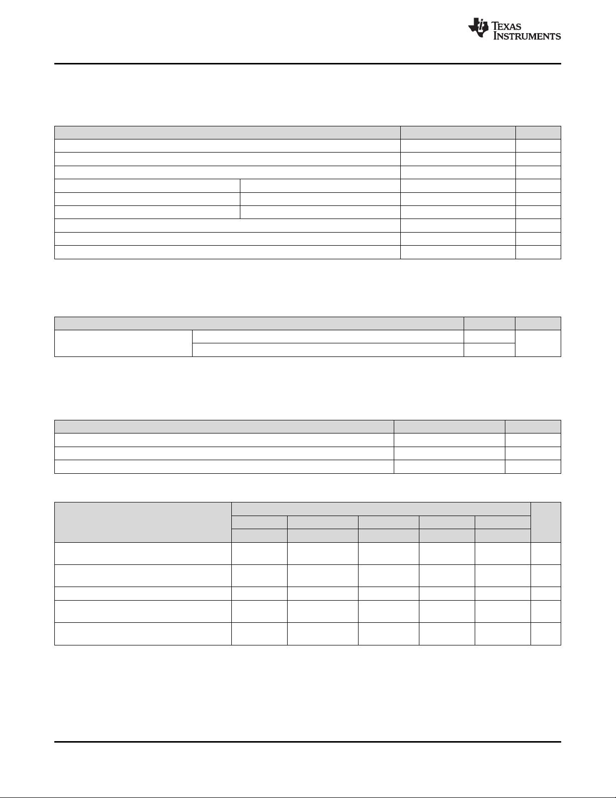
Device Information
(1)
PART NUMBER PACKAGE BODY SIZE (NOM)
SN74LV4046ANS SO (16) 7.70 mm × 10.20 mm
SN74LV4046AD SOIC (16) 6.00 mm × 9.90 mm
SN74LV4046APW TSSOP (16) 6.40 mm × 5.00 mm
SN74LV4046ADGVR TVSOP (16) 3.60 mm × 4.40 mm
SN74LV4046AN PDIP (16) 19.30 mm × 6.35 mm
(1) For all available packages, see the orderable addendum at
the end of the data sheet.
SN74LV4046A Functional Block Diagram

剩余26页未读,继续阅读


评论0
最新资源