没有合适的资源?快使用搜索试试~ 我知道了~
TI-SN74HCT595-Q1.pdf
需积分: 5 1 下载量 191 浏览量
2022-11-27
23:01:20
上传
评论 4
收藏 1.17MB PDF 举报
温馨提示
试读
29页
TI-SN74HCT595-Q1.pdf
资源详情
资源评论
SN74HCT595-Q1 Automotive 8-Bit Shift Registers with 3-State Output Registers
1 Features
• AEC-Q100 Qualified for automotive applications:
– Device temperature grade 1:
• –40°C to +125°C, T
A
– Device HBM ESD Classification Level 2
– Device CDM ESD Classifcation Level C6
• LSTTL input logic compatible
– V
IL(max)
= 0.8 V, V
IH(min)
= 2 V
• CMOS input logic compatible
– I
I
≤ 1 µA at V
OL
, V
OH
• 4.5 V to 5.5 V operation
• Supports fanout up to 10 LSTTL loads
• Shift register has direct clear
2 Applications
• Output expansion
• LED matrix control
• 7-segment display control
• 8-bit data storage
3 Description
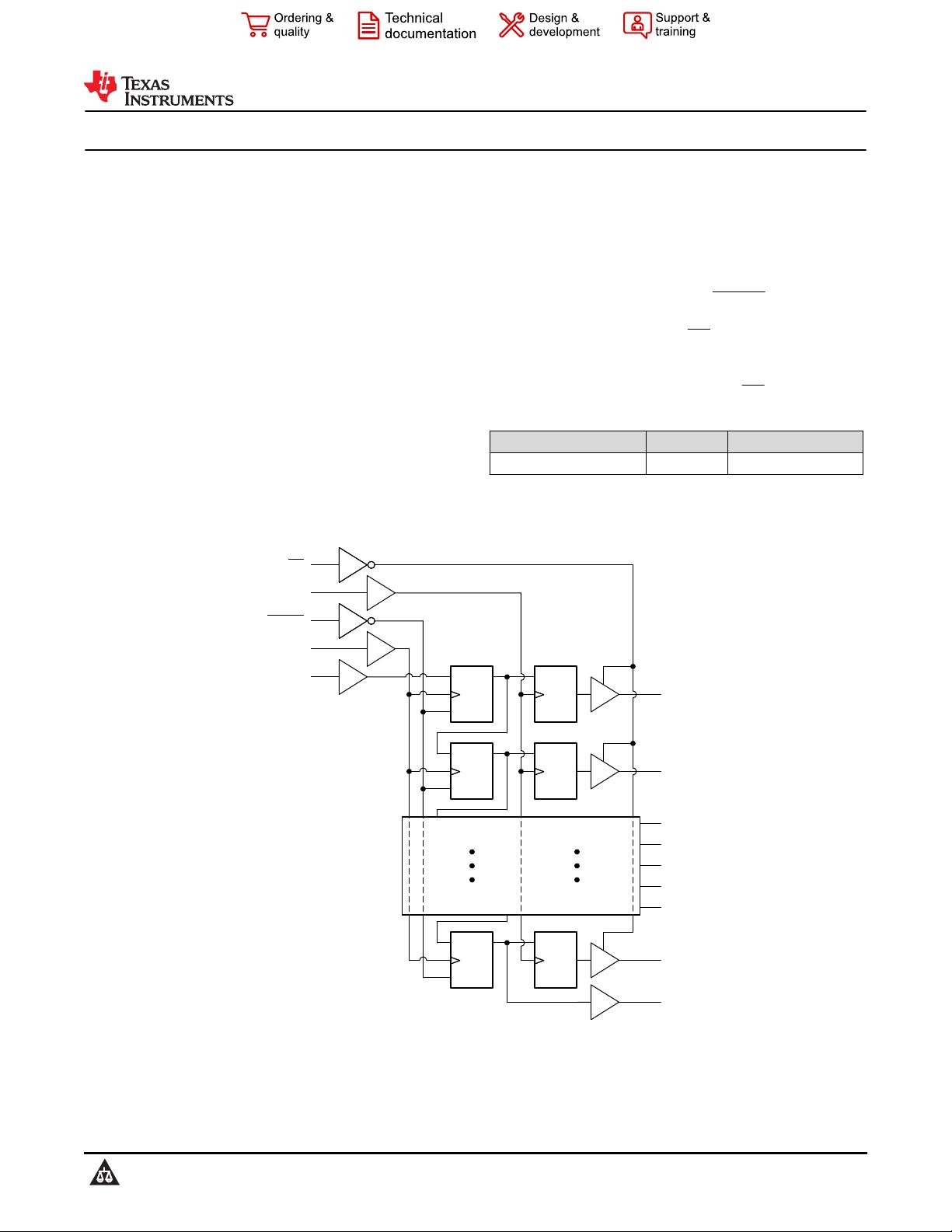
The SN74HCT595-Q1 device contains an 8-bit, serial-
in, parallel-out shift register that feeds an 8-bit D-type
storage register. The storage register has parallel
3-state outputs. Separate clocks are provided for
both the shift and storage register. The shift register
has a direct overriding clear (SRCLR) input, serial
(SER) input, and a serial output (Q
H'
) for cascading.
When the output-enable (OE) input is high, the
storage register outputs are in a high-impedance
state. Internal register data and serial output (Q
H'
) are
not impacted by the operation of the OE input.
Device Information
(1)
PART NUMBER PACKAGE BODY SIZE (NOM)
SN74HCT595PW-Q1 TSSOP (16) 5.00 mm × 4.40 mm
(1) For all available packages, see the orderable addendum at
the end of the data sheet.
RCLK
OE
SRCLR
SRCLK
SER
13
12
10
11
14
D
R
15
1
Q
A
Q
B
Q
C
Q
D
R
Q
D
Q
D
Q
2
Q
D
3
Q
E
4
Q
F
5
Q
G
6
D
R
7
9
Q
H’
Q
D
Q Q
H
Logic Diagram (Positive Logic)
ADVANCE INFORMATION
SN74HCT595-Q1
SCLS883 – OCTOBER 2021
An IMPORTANT NOTICE at the end of this data sheet addresses availability, warranty, changes, use in safety-critical applications,
intellectual property matters and other important disclaimers. ADVANCE INFORMATION for preproduction products; subject to change
without notice.
Table of Contents
1 Features............................................................................1
2 Applications..................................................................... 1
3 Description.......................................................................1
4 Revision History.............................................................. 2
5 Pin Configuration and Functions...................................3
6 Specifications.................................................................. 4
6.1 Absolute Maximum Ratings........................................ 4
6.2 ESD Ratings............................................................... 4
6.3 Recommended Operating Conditions.........................4
6.4 Thermal Information....................................................4
6.5 Electrical Characteristics.............................................5
6.6 Timing Characteristics.................................................5
6.7 Switching Characteristics............................................6
6.8 Typical Characteristics................................................ 8
7 Parameter Measurement Information............................ 9
8 Detailed Description......................................................10
8.1 Functional Block Diagram......................................... 10
8.2 Feature Description...................................................10
8.3 Device Functional Modes..........................................12
9 Application and Implementation.................................. 13
9.1 Application Information............................................. 13
9.2 Typical Application.................................................... 14
10 Power Supply Recommendations..............................17
11 Layout........................................................................... 17
11.1 Layout Guidelines................................................... 17
11.2 Layout Example...................................................... 17
12 Device and Documentation Support..........................18
12.1 Documentation Support.......................................... 18
12.2 Receiving Notification of Documentation Updates..18
12.3 Support Resources................................................. 18
12.4 Trademarks............................................................. 18
12.5 Electrostatic Discharge Caution..............................18
12.6 Glossary..................................................................18
13 Mechanical, Packaging, and Orderable
Information.................................................................... 18
13.1 Tape and Reel Information......................................22
4 Revision History
DATE REVISION NOTES
October 2021 * Initial Release
SN74HCT595-Q1
SCLS883 – OCTOBER 2021
www.ti.com
ADVANCE INFORMATION
2 Submit Document Feedback
Copyright © 2021 Texas Instruments Incorporated
Product Folder Links: SN74HCT595-Q1
5 Pin Configuration and Functions
1
2
3
7
4
5
6
14
13
12
8
11
10
9
GND
SER
RCLK
SRCLK
V
CC
15
16
Q
B
Q
C
Q
D
Q
E
Q
F
Q
G
Q
H
Q
A
OE
SRCLR
Q
H
PW Package
16-Pin TSSOP
Top View
Table 5-1. Pin Functions
PIN
TYPE DESCRIPTION
NAME NO.
Q
B
1 Output Q
B
output
Q
C
2 Output Q
C
output
Q
D
3 Output Q
D
output
Q
E
4 Output Q
E
output
Q
F
5 Output Q
F
output
Q
G
6 Output Q
G
output
Q
H
7 Output Q
H
output
GND 8 — Ground
Q
H'
9 Output Serial output, can be used for cascading
SRCLR 10 Input Shift register clear, active low
SRCLK 11 Input Shift register clock, rising edge triggered
RCLK 12 Input Output register clock, rising edge triggered
OE 13 Input Output Enable, active low
SER 14 Input Serial input
Q
A
15 Output Q
A
output
V
CC
16 — Positive supply
www.ti.com
SN74HCT595-Q1
SCLS883 – OCTOBER 2021
ADVANCE INFORMATION
Copyright © 2021 Texas Instruments Incorporated
Submit Document Feedback
3
Product Folder Links: SN74HCT595-Q1
6 Specifications
6.1 Absolute Maximum Ratings
over operating free-air temperature range (unless otherwise noted)
(1)
MIN MAX UNIT
V
CC
Supply voltage –0.5 7 V
I
IK
Input clamp current
(2)
V
I
< 0 or V
I
>V
CC
+ 0.5 V –20 20 mA
I
OK
Output clamp current
(2)
V
O
< 0 or V
O
> V
CC
+ 0.5
V
–20 20 mA
I
O
Continuous output current V
O
= 0 to V
CC
–35 35 mA
I
CC
Continuous output current through V
CC
or GND –70 70 mA
T
J
Junction temperature 150 °C
T
stg
Storage temperature –65 150 °C
(1) Stresses beyond those listed under Absolute Maximum Rating may cause permanent damage to the device. These are stress
ratings only, which do not imply functional operation of the device at these or any other conditions beyond those indicated
under Recommended Operating Condition. Exposure to absolute-maximum-rated conditions for extended periods may affect device
reliability.
(2) The input and output voltage ratings may be exceeded if the input and output current ratings are observed.
6.2 ESD Ratings
VALUE UNIT
V
(ESD)
Electrostatic discharge
Human body model (HBM), per AEC Q100-002
(1)
HBM ESD Classification Level 2
±4000
V
Charged device model (CDM), per AEC
Q100-011
CDM ESD Classification Level C4B
±1500
(1) AEC Q100-002 indicate that HBM stressing shall be in accordrance with the ANSI/ESDA/JEDEC JS-001 specification.
6.3 Recommended Operating Conditions
over operating free-air temperature range (unless otherwise noted)
MIN NOM MAX UNIT
V
CC
Supply voltage 4.5 5 5.5 V
V
IH
High-level input voltage V
CC
= 4.5 V to 5.5V 2 V
V
IL
Low-level input voltage V
CC
= 4.5 V to 5.5V 0.8 V
V
I
Input voltage 0 V
CC
V
V
O
Output voltage 0 V
CC
V
Δt/Δv Input transition rise and fall rate V
CC
= 4.5 V to 5.5V 500 ns/V
T
A
Ambient temperature –40 125 °C
6.4 Thermal Information
THERMAL METRIC
(1)
SN74HCT595-Q1
UNITPW (TSSOP)
16 PINS
R
θJA
Junction-to-ambient thermal resistance 131.8 °C/W
R
θJC(top)
Junction-to-case (top) thermal resistance 69.8 °C/W
R
θJB
Junction-to-board thermal resistance 76.5 °C/W
Ψ
JT
Junction-to-top characterization parameter 20.9 °C/W
Y
JB
Junction-to-board characterization parameter 76.1 °C/W
SN74HCT595-Q1
SCLS883 – OCTOBER 2021
www.ti.com
ADVANCE INFORMATION
4 Submit Document Feedback
Copyright © 2021 Texas Instruments Incorporated
Product Folder Links: SN74HCT595-Q1
6.4 Thermal Information (continued)
THERMAL METRIC
(1)
SN74HCT595-Q1
UNITPW (TSSOP)
16 PINS
R
θJC(bot)
Junction-to-case (bottom) thermal resistance N/A °C/W
(1) For more information about traditional and new thermal metrics, see the Semiconductor and IC Package Thermal Metrics application
report.
6.5 Electrical Characteristics
over operating free-air temperature range (unless otherwise noted)
PARAMETER TEST CONDITIONS
T
A
= 25°C -40°C to 125°C
UNIT
MIN TYP MAX MIN TYP MAX
V
OH
High-level output voltage V
I
= V
IH
or V
IL
I
OH
= -20 uA, V
CC
=
4.5 V
4.4 4.4 V
I
OH
= -6 mA, V
CC
=
4.5 V
3.98 3.84 V
I
OH
= -4 mA, V
CC
=
4.5 V
3.98 3.84 V
V
OL
Low-level output voltage V
I
= V
IH
or V
IL
I
OL
= 20 uA, V
CC
=
4.5 V
0.1 0.1 V
I
OL
= 4 mA, V
CC
=
4.5 V
0.26 0.33 V
I
OL
= 6 mA, V
CC
=
4.5 V
0.26 0.33 V
I
I
Input leakage current V
I
= V
CC
or 0 V
CC
= 5.5 V ±100
±100
0
nA
I
OZ
Off-State (High-Impedance State) Output
Current
V
O
= V
CC
or 0, Q
A
-
Q
H
V
CC
= 5.5 V ±0.5 ±5 µA
I
CC
Supply current V
I
= V
CC
or 0, I
O
= 0 V
CC
= 5.5 V 8 80 µA
ΔI
CC
Additional Quiescent Device Current Per
Input Pin
V
I
= V
CC
- 2.1V V
CC
= 4.5V to 5.5V
126.
2
157.
5
µA
V
I
= 0.5 V or 2.4V V
CC
= 5.5V 2.4 2.9 mA
C
i
Input capacitance V
CC
= 4.5V to 5.5V V
CC
= 4.5V to 5.5V 10 pF
C
O
Output capacitance V
CC
= 4.5V to 5.5V V
CC
= 4.5V to 5.5V 20 pF
C
pd
Power dissipation capacitance per gate No load 50 pF
6.6 Timing Characteristics
over recommended operating free-air temperature range (unless otherwise noted)
PARAMETER CONDITION V
CC
T
A
= 25°C -40°C to 125°C
UNIT
MIN MAX MIN MAX
f
clock
Clock frequency 4.5 V 31 25 MHz
t
w
Pulse duration
SRCLK or RCLK high or low
4.5 V 16 20
ns
5.5 V 16 20
SRCLR low
4.5 V 16 20
5.5 V 16 20
www.ti.com
SN74HCT595-Q1
SCLS883 – OCTOBER 2021
ADVANCE INFORMATION
Copyright © 2021 Texas Instruments Incorporated
Submit Document Feedback
5
Product Folder Links: SN74HCT595-Q1
剩余28页未读,继续阅读
安全验证
文档复制为VIP权益,开通VIP直接复制
信息提交成功
评论0
最新资源