没有合适的资源?快使用搜索试试~ 我知道了~
TI-CD74HCT4046A.pdf
需积分: 5 0 下载量 144 浏览量
2022-11-30
23:37:59
上传
评论 4
收藏 1.15MB PDF 举报
温馨提示
试读
34页
TI-CD74HCT4046A.pdf
资源推荐
资源详情
资源评论
1
Data sheet acquired from Harris Semiconductor
SCHS204J
Features
• Operating Frequency Range
- Up to 18MHz (Typ) at V
CC
= 5V
- Minimum Center Frequency of 12MHz at V
CC
= 4.5V
• Choice of Three Phase Comparators
- EXCLUSIVE-OR
- Edge-Triggered JK Flip-Flop
- Edge-Triggered RS Flip-Flop
• Excellent VCO Frequency Linearity
• VCO-Inhibit Control for ON/OFF Keying and for Low
Standby Power Consumption
• Minimal Frequency Drift
• Operating Power Supply Voltage Range
- VCO Section . . . . . . . . . . . . . . . . . . . . . . . . . . 3V to 6V
- Digital Section . . . . . . . . . . . . . . . . . . . . . . . . 2V to 6V
• Fanout (Over Temperature Range)
- Standard Outputs. . . . . . . . . . . . . . . 10 LSTTL Loads
- Bus Driver Outputs . . . . . . . . . . . . . 15 LSTTL Loads
• Wide Operating Temperature Range . . . -55
o
C to 125
o
C
• Balanced Propagation Delay and Transition Times
• Significant Power Reduction Compared to LSTTL
Logic ICs
• HC Types
- 2V to 6V Operation
- High Noise Immunity: N
IL
= 30%, N
IH
= 30% of V
CC
at V
CC
= 5V
• HCT Types
- 4.5V to 5.5V Operation
- Direct LSTTL Input Logic Compatibility,
V
IL
= 0.8V (Max), V
IH
= 2V (Min)
- CMOS Input Compatibility, I
l
≤ 1µA at VOL, VOH
Applications
• FM Modulation and Demodulation
• Frequency Synthesis and Multiplication
• Frequency Discrimination
• Tone Decoding
• Data Synchronization and Conditioning
• Voltage-to-Frequency Conversion
• Motor-Speed Control
Description
The ’HC4046A and ’HCT4046A are high-speed silicon-gate
CMOS devices that are pin compatible with the CD4046B of
the “4000B” series. They are specified in compliance with
JEDEC standard number 7.
The ’HC4046A and ’HCT4046A are phase-locked-loop
circuits that contain a linear voltage-controlled oscillator
(VCO) and three different phase comparators (PC1, PC2 and
PC3). A signal input and a comparator input are common to
each comparator.
The signal input can be directly coupled to large voltage
signals, or indirectly coupled (with a series capacitor) to small
voltage signals. A self-bias input circuit keeps small voltage
signals within the linear region of the input amplifiers. With a
passive low-pass filter, the 4046A forms a second-order loop
PLL. The excellent VCO linearity is achieved by the use of
linear op-amp techniques.
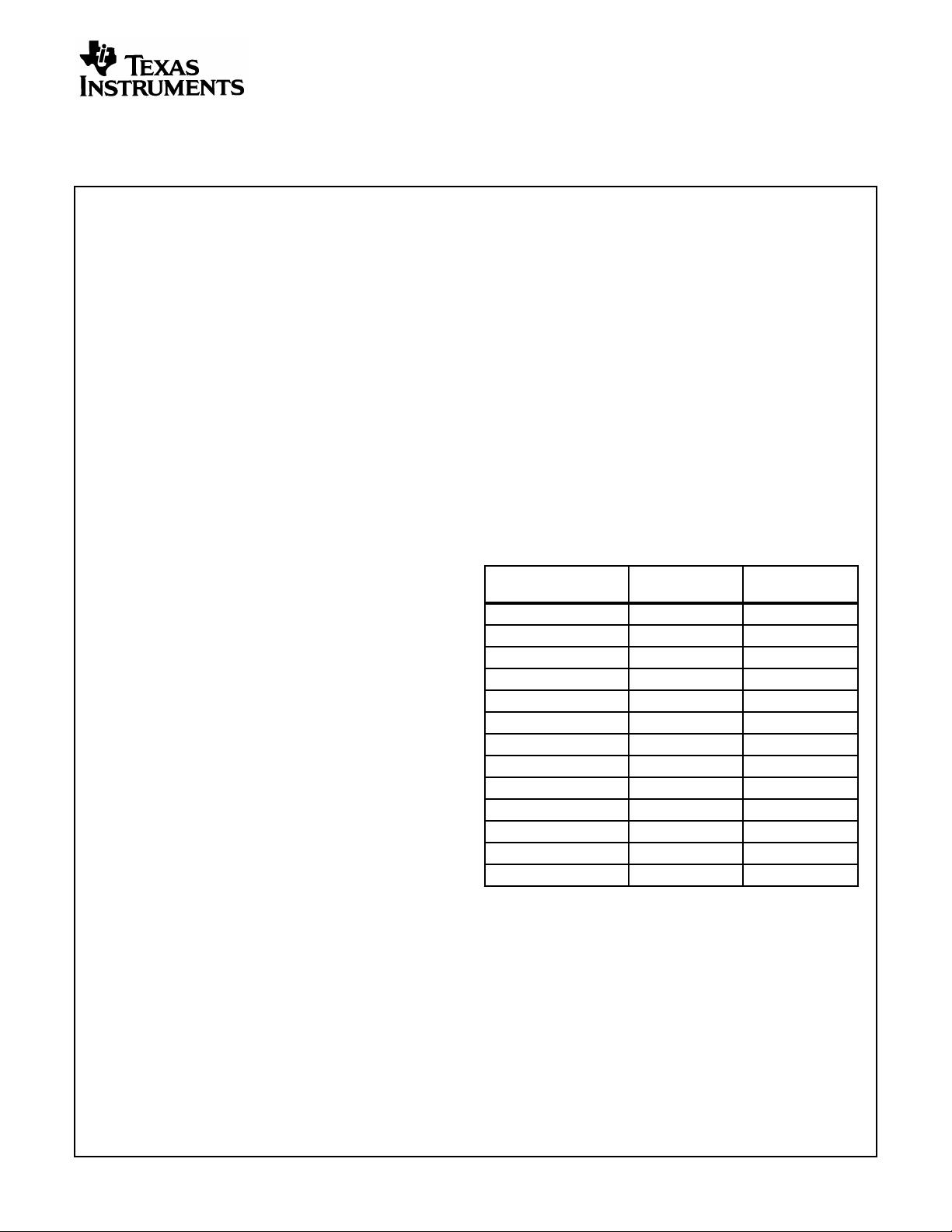
Ordering Information
PART NUMBER
TEMP. RANGE
(
o
C) PACKAGE
CD54HC4046AF3A -55 to 125 16 Ld CERDIP
CD54HCT4046AF3A -55 to 125 16 Ld CERDIP
CD74HC4046AE -55 to 125 16 Ld PDIP
CD74HC4046AM -55 to 125 16 Ld SOIC
CD74HC4046AMT -55 to 125 16 Ld SOIC
CD74HC4046AM96 -55 to 125 16 Ld SOIC
CD74HC4046ANSR -55 to 125 16 Ld SOP
CD74HC4046APWR -55 to 125 16 Ld TSSOP
CD74HC4046APWT -55 to 125 16 Ld TSSOP
CD74HCT4046AE -55 to 125 16 Ld PDIP
CD74HCT4046AM -55 to 125 16 Ld SOIC
CD74HCT4046AMT -55 to 125 16 Ld SOIC
CD74HCT4046AM96 -55 to 125 16 Ld SOIC
NOTE: When ordering, use the entire part number. The suffixes 96
and R denote tape and reel. The suffix T denotes a small-quantity
reel of 250.
February 1998 - Revised December 2003
CAUTION: These devices are sensitive to electrostatic discharge. Users should follow proper IC Handling Procedures.
Copyright
© 2003, Texas Instruments Incorporated
CD54HC4046A, CD74HC4046A,
CD54HCT4046A, CD74HCT4046A
High-Speed CMOS Logic
Phase-Locked Loop with VCO
[ /Title
(CD74
HC404
6A,
CD74
HCT40
46A)
/Sub-
ject
(High-
Speed
CMOS
2
Pinout
CD54HC4046A, CD54HCT4046A (CERDIP)
CD74HC4046A (PDIP, SOIC, SOP, TSSOP)
CD74HCT4046A (PDIP, SOIC)
TOP VIEW
Functional Diagram
14
15
16
9
13
12
11
10
1
2
3
4
5
7
6
8
PCP
OUT
PC1
OUT
COMP
IN
VCO
OUT
INH
C1
A
GND
C1
B
V
CC
SIG
IN
PC2
OUT
R
2
R
1
DEM
OUT
VCO
IN
PC3
OUT
10
4
VCO
OUT
DEM
OUT
5
6
7
12
C1
A
R
1
VCO
IN
INH
9
11
C1
B
R
2
15
1
13
2
PC1
OUT
PC3
OUT
PC2
OUT
PCP
OUT
14
3
COMP
IN
SIG
IN
φ
VCO
Pin Descriptions
PIN NUMBER SYMBOL NAME AND FUNCTION
1 PCP
OUT
Phase Comparator Pulse Output
2 PC1
OUT
Phase Comparator 1 Output
3 COMP
IN
Comparator Input
4 VCO
OUT
VCO Output
5 INH Inhibit Input
6C1
A
Capacitor C1 Connection A
7C1
B
Capacitor C1 Connection B
8 GND Ground (0V)
9 VCO
IN
VCO Input
10 DEM
OUT
Demodulator Output
11 R
1
Resistor R1 Connection
12 R
2
Resistor R2 Connection
13 PC2
OUT
Phase Comparator 2 Output
14 SIG
IN
Signal Input
15 PC3
OUT
Phase Comparator 3 Output
16 V
CC
Positive Supply Voltage
CD54HC4046A, CD74HC4046A, CD54HCT4046A, CD74HCT4046ACD54HC4046A, CD74HC4046A, CD54HCT4046A, CD74HCT4046A
3
General Description
VCO
The VCO requires one external capacitor C1 (between C1
A
and C1
B
) and one external resistor R1 (between R
1
and
GND) or two external resistors R1 and R2 (between R
1
and
GND, and R
2
and GND). Resistor R1 and capacitor C1
determine the frequency range of the VCO. Resistor R2
enables the VCO to have a frequency offset if required. See
logic diagram, Figure 1.
The high input impedance of the VCO simplifies the design
of low-pass filters by giving the designer a wide choice of
resistor/capacitor ranges. In order not to load the low-pass
filter, a demodulator output of the VCO input voltage is
provided at pin 10 (DEM
OUT
). In contrast to conventional
techniques where the DEM
OUT
voltage is one threshold
voltage lower than the VCO input voltage, here the DEM
OUT
voltage equals that of the VCO input. If DEM
OUT
is used, a
load resistor (R
S
) should be connected from DEM
OUT
to
GND; if unused, DEM
OUT
should be left open. The VCO
output (VCO
OUT
) can be connected directly to the
comparator input (COMP
IN
), or connected via a frequency-
divider. The VCO output signal has a specified duty factor of
50%. A LOW level at the inhibit input (INH) enables the VCO
and demodulator, while a HIGH level turns both off to
minimize standby power consumption.
Phase Comparators
The signal input (SIG
IN
) can be directly coupled to the self-
biasing amplifier at pin 14, provided that the signal swing is
between the standard HC family input logic levels.
Capacitive coupling is required for signals with smaller
swings.
Phase Comparator 1 (PC1)
This is an Exclusive-OR network. The signal and comparator
input frequencies (f
i
) must have a 50% duty factor to obtain
the maximum locking range. The transfer characteristic of
PC1, assuming ripple (f
r
= 2f
i
) is suppressed, is:
V
DEMOUT
=(V
CC
/π)(φSIG
IN
- φCOMP
IN
) where V
DEMOUT
is the demodulator output at pin 10; V
DEMOUT
=V
PC1OUT
(via low-pass filter).
The average output voltage from PC1, fed to the VCO input
via the low-pass filter and seen at the demodulator output at
pin 10 (V
DEMOUT
), is the resultant of the phase differences
of signals (SIG
IN
) and the comparator input (COMP
IN
)as
shown in Figure 2. The average of V
DEM
is equal to 1/2
V
CC
when there is no signal or noise at SIG
IN
, and with this
input the VCO oscillates at the center frequency (f
o
).
Typical waveforms for the PC1 loop locked at f
o
are shown
in Figure 3.
FIGURE 1. LOGIC DIAGRAM
DEM
OUT
R2
12
R1
R5
11
10
C1
R3
C2
PC2
OUT
13
p
n
GND
V
CC
PCP
OUT
1
15
2
PC3
OUT
PC1
OUT
DOWN
R
D
Q
Q
D
CP
R
D
Q
Q
D
CP
UP
V
CC
V
CC
R
D
Q
Q
S
D
INH
59
VCO
IN
VCO
-
+
VCO
OUT
COMP
IN
-
+
SIG
IN
C1
B
C1
A
V
REF
R2
R1
674314
-
+
CD54HC4046A, CD74HC4046A, CD54HCT4046A, CD74HCT4046ACD54HC4046A, CD74HC4046A, CD54HCT4046A, CD74HCT4046A
4
The frequency capture range (2f
C
) is defined as the
frequency range of input signals on which the PLL will lock if
it was initially out-of-lock. The frequency lock range (2f
L
)is
defined as the frequency range of input signals on which the
loop will stay locked if it was initially in lock. The capture
range is smaller or equal to the lock range.
With PC1, the capture range depends on the low-pass filter
characteristics and can be made as large as the lock range.
This configuration retains lock behavior even with very noisy
input signals. Typical of this type of phase comparator is that
it can lock to input frequencies close to the harmonics of the
VCO center frequency.
Phase Comparator 2 (PC2)
This is a positive edge-triggered phase and frequency
detector. When the PLL is using this comparator, the loop
is controlled by positive signal transitions and the duty
factors of SIG
IN
and COMP
IN
are not important. PC2
comprises two D-type flip-flops, control-gating and a three-
state output stage. The circuit functions as an up-down
counter (Figure 1) where SIG
IN
causes an up-count and
COMP
IN
a down-count. The transfer function of PC2,
assuming ripple (f
r
= f
i
) is suppressed, is:
V
DEMOUT
=(V
CC
/4π)(φSIG
IN
- φCOMP
IN
) where
V
DEMOUT
is the demodulator output at pin 10;
V
DEMOUT
=V
PC2OUT
(via low-pass filter).
The average output voltage from PC2, fed to the VCO via the
low-pass filter and seen at the demodulator output at pin 10
(V
DEMOUT
), is the resultant of the phase differences of
SIG
IN
and COMP
IN
as shown in Figure 4. Typical waveforms
for the PC2 loop locked at f
o
are shown in Figure 5.
When the frequencies of SIG
IN
and COMP
IN
are equal but
the phase of SIG
IN
leads that of COMP
IN
, the p-type output
driver at PC2
OUT
is held “ON” for a time corresponding to
the phase difference (φ
DEMOUT
). When the phase of SIG
IN
lags that of COMP
IN
, the n-type driver is held “ON”.
When the frequency of SIG
IN
is higher than that of
COMP
IN
, the p-type output driver is held “ON” for most of
the input signal cycle time, and for the remainder of the
cycle both n- and p-type drivers are “OFF” (three-state). If
the SIG
IN
frequency is lower than the COMP
IN
frequency,
then it is the n-type driver that is held “ON” for most of the
cycle. Subsequently, the voltage at the capacitor (C2) of
the low-pass filter connected to PC2
OUT
varies until the
signal and comparator inputs are equal in both phase and
FIGURE 2. PHASE COMPARATOR 1: AVERAGE OUTPUT
VOLTAGE vs INPUT PHASE DIFFERENCE:
V
DEMOUT
= V
PC1OUT
= (V
CC
/π) (φSIG
IN
-
φCOMP
IN
); φ
DEMOUT
=(φSIG
IN
- φCOMP
IN
)
V
CC
V
DEMOUT (AV)
1/2 V
CC
0
0
o
90
o
φ
DEMOUT
180
o
FIGURE 3. TYPICAL WAVEFORMS FOR PLL USING PHASE
COMPARATOR 1, LOOP LOCKED AT f
o
SIG
IN
COMP
IN
VCO
OUT
PC1
OUT
VCO
IN
V
CC
GND
FIGURE 4. PHASE COMPARATOR 2: AVERAGE OUTPUT
VOLTAGE vs INPUT PHASE DIFFERENCE:
V
DEMOUT
= V
PC2OUT
= (V
CC
/4π) (φSIG
IN
- φCOMP
IN
);
φ
DEMOUT
=(φSIG
IN
- φCOMP
IN
)
V
CC
V
DEMOUT (AV)
1/2 V
CC
0
-360
o
0
o
φ
DEMOUT
360
o
FIGURE 5. TYPICAL WAVEFORMS FOR PLL USING PHASE
COMPARATOR 2, LOOP LOCKED AT f
o
SIG
IN
COMP
IN
VCO
OUT
PC2
OUT
VCO
IN
V
CC
GND
PCP
OUT
HIGH IMPEDANCE OFF - STATE
CD54HC4046A, CD74HC4046A, CD54HCT4046A, CD74HCT4046ACD54HC4046A, CD74HC4046A, CD54HCT4046A, CD74HCT4046A
5
frequency. At this stable point the voltage on C2 remains
constant as the PC2 output is in three-state and the VCO
input at pin 9 is a high impedance. Also in this condition,
the signal at the phase comparator pulse output (PCP
OUT
)
is a HIGH level and so can be used for indicating a locked
condition.
Thus, for PC2, no phase difference exists between SIG
IN
and COMP
IN
over the full frequency range of the VCO.
Moreover, the power dissipation due to the low-pass filter is
reduced because both p- and n-type drivers are “OFF” for
most of the signal input cycle. It should be noted that the
PLL lock range for this type of phase comparator is equal to
the capture range and is independent of the low-pass filter.
With no signal present at SIG
IN
, the VCO adjusts, via PC2,
to its lowest frequency.
Phase Comparator 3 (PC3)
This is a positive edge-triggered sequential phase
detector using an RS-type flip-flop. When the PLL is using
this comparator, the loop is controlled by positive signal
transitions and the duty factors of SIG
IN
and COMP
IN
are
not important. The transfer characteristic of PC3,
assuming ripple (f
r
= f
i
) is suppressed, is:
V
DEMOUT
=(V
CC
/2p) (fSIG
IN
- fCOMP
IN
) where
V
DEMOUT
is the demodulator output at pin 10; V
DEMOUT
= V
PC3OUT
(via low-pass filter).
The average output from PC3, fed to the VCO via the low-
pass filter and seen at the demodulator at pin 10
(V
DEMOUT
), is the resultant of the phase differences of
SIG
IN
and COMP
IN
as shown in Figure 6. Typical
waveforms for the PC3 loop locked at f
o
are shown in
Figure 7.
The phase-to-output response characteristic of PC3
(Figure 6) differs from that of PC2 in that the phase angle
between SIG
IN
and COMP
IN
varies between 0
o
and 360
o
and is 180
o
at the center frequency. Also PC3 gives a
greater voltage swing than PC2 for input phase differences
but as aconsequence the ripple content of the VCO input
signal is higher. With no signal present at SIG
IN
, the VCO
adjusts, via PC3, to its highest frequency.
The only difference between the HC and HCT versions is the
input level specification of the INH input. This input disables
the VCO section. The comparator’s sections are identical, so
that there is no difference in the SIG
IN
(pin 14) or COMP
IN
(pin 3) inputs between the HC and the HCT versions.
FIGURE 6. PHASE COMPARATOR 3: AVERAGE OUTPUT
VOLTAGE vs INPUT PHASE DIFFERENCE:
V
DEMOUT
= V
PC3OUT
= (V
CC
/2π) (φSIG
IN
- φCOMP
IN
);
φ
DEMOUT
= (φSIG
IN
- φCOMP
IN
)
V
CC
V
DEMOUT (AV)
1/2 V
CC
0
0
o
180
o
φ
DEMOUT
360
o
FIGURE 7. TYPICAL WAVEFORMS FOR PLL USING PHASE
COMPARATOR 3, LOOP LOCKED AT f
o
SIG
IN
COMP
IN
VCO
OUT
PC3
OUT
VCO
IN
V
CC
GND
CD54HC4046A, CD74HC4046A, CD54HCT4046A, CD74HCT4046A
剩余33页未读,继续阅读
资源评论
不觉明了
- 粉丝: 3153
- 资源: 5416
上传资源 快速赚钱
- 我的内容管理 展开
- 我的资源 快来上传第一个资源
- 我的收益 登录查看自己的收益
- 我的积分 登录查看自己的积分
- 我的C币 登录后查看C币余额
- 我的收藏
- 我的下载
- 下载帮助
最新资源
- python开心麻花影视作品分析程序+源码.zip
- pythonExcel数据分析师程序+源码.zip
- PlatformUI.jar 支持RCP控件环境插件
- 基于BP神经网络的回归分析,基于优化动量因子的BP神经网络,基于优化学习率的BP神经网络,基于优化隐藏层神经元的bp神经网络
- python读取excel数据Python-file-reading-master.zip
- STC15单片机串口2使用程序例子
- 读取日志的excel生成周报 用python3开发weekplan-master.zip
- python 读取excel数据导入dbimport-data-master.zip
- K折交叉验证BP神经网络,多输入多输出BP神经网络(代码完整,数据齐全)
- B07训练原图.zip
资源上传下载、课程学习等过程中有任何疑问或建议,欢迎提出宝贵意见哦~我们会及时处理!
点击此处反馈
安全验证
文档复制为VIP权益,开通VIP直接复制
信息提交成功