TI-ADS8686S.pdf
需积分: 5 67 浏览量
2022-11-27
00:07:04
上传
评论 4
收藏 1.72MB PDF 举报

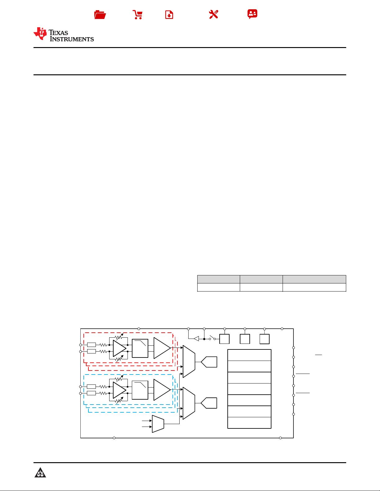
DGNDAGND
DVDD
AVDD
ADC
Driver
Serial - Parallel -
Byte Interface
1 M
Clamp
2
nd
Order
PROG
LPF
Clamp
PGA
AIN_nA
AIN_nAGND
1 M
9:1
MUX
2:1
MUX
AVDD
ALDO
ADS8686S
16-BIT
SAR
REFIO REFSEL REGCAP
ALDO
2.5 V
REF
REGCAPD
DLDO
REFCAP
CH0A
CH7A
ADC
Driver
1 M
Clamp
2
nd
Order
PROG
LPF
Clamp
PGA
AIN_nB
AIN_nBGND
1 M
9:1
MUX
CH0B
CH7B
16-BIT
SAR
Digital OSR Filter
Channel Sequencer
Burst Capture
CRC
Self Diagnosys
Dual Simultaneous
Sampling
DB[15:0]
SER/BYTE/PAR
SDOx/SDI
SER1W
OSR
RESET
CONVST
BUSY
Product
Folder
Order
Now
Technical
Documents
Tools &
Software
Support &
Community
An IMPORTANT NOTICE at the end of this data sheet addresses availability, warranty, changes, use in safety-critical applications,
intellectual property matters and other important disclaimers. PRODUCTION DATA.
ADS8686S
SBAS905C –NOVEMBER 2019–REVISED JULY 2020
ADS8686S 16-Channel, 16-Bit, 1-MSPS, Dual, Simultaneous Sampling ADC with Integrated
Analog Front-End
1
1 Features
1
• 16-channel, 16-bit ADC with integrated analog
front-end
• Dual simultaneous sampling: 8x2 channels
• Supply:
– Analog: 5 V
– Digital: 1.8 V to 5 V
• Constant 1-MΩ input impedance front-end
• Independently programmable input ranges with
20% overrange
• Programmable low-pass filter:
– 15 kHz, 39 kHz, 376 kHz
• Excellent DC and AC performance
• On-chip reference and reference buffer
• Excellent over temperature performance
• Overvoltage input clamp with 8-kV ESD
• Optional cyclic redundancy check (CRC) error
checking
• On-chip self diagnostic function
• Temperature range: –40°C to +125°C
2 Applications
• Multifunction relays
• Servo drive position sensors
• Analog input modules
• Data acquisition (DAQ)
3 Description
The ADS8686S is a 16-channel data acquisition
(DAQ) system based on a dual simultaneous-
sampling, 16-bit successive approximation register
(SAR) analog-to-digital converter (ADC). The
ADS8686S features a complete analog front-end for
each channel with an input clamp, 1-MΩ input
impedance, independently programmable gain
amplifier (PGA), programmable low-pass filter, and an
ADC input driver. The device also features a low-drift,
precision reference with a buffer to drive the ADCs. A
flexible digital interface supporting serial, parallel, and
byte communication enables the device to be used
with a variety of host controllers.
The ADS8686S can be configured to accept ±10-V,
±5-V, or ±2.5-V bipolar inputs with a 20% overrange
option using a single 5-V supply. The high input
impedance allows direct connection with sensors and
transformers, thus eliminating the need for external
driver circuits. The ADS8686S has a highly
configurable channel sequencer to reduce the
sequencing overhead on the backend controller or
processor. The high performance and accuracy,
along with zero-latency conversions offered by this
device make the ADS8686S a great choice for
multiple industrial applications.
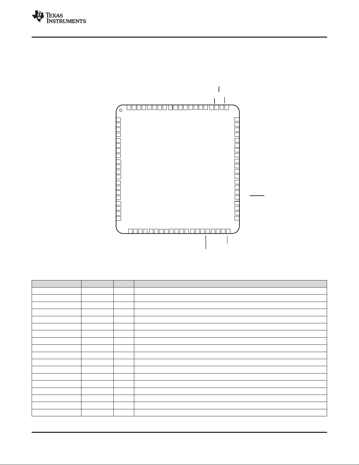
Device Information
(1)
PART NUMBER PACKAGE BODY SIZE (NOM)
ADS8686S LQFP (80) 14.00 mm x 14.00 mm
(1) For all available packages, see the orderable addendum at
the end of the data sheet.
Device Block Diagram


剩余101页未读,继续阅读
资源评论


