没有合适的资源?快使用搜索试试~ 我知道了~
TI-ADS131M06.pdf
需积分: 5 0 下载量 63 浏览量
2022-11-27
00:08:07
上传
评论 4
收藏 3.9MB PDF 举报
温馨提示
试读
109页
TI-ADS131M06.pdf
资源推荐
资源详情
资源评论
ADS131M06 6 通道、同步采样、24 位 Δ-Σ ADC
1 特性
• 6 同步采样差分输入
• 可编程数据速率高达 32kSPS
• 可编程增益高达 128
• 噪声性能:
– 当增益为 1.4kSPS 时,动态范围为 102dB
– 当增益为 64.4kSPS 时,动态范围为 80dB
• 总谐波失真:-100dB
• 用于直接传感器连接的高阻抗输入:
– 当增益为 1、2 和 4 时,
输入阻抗为 330kΩ
– 当增益为 8、16、32、64 和 128 时,
输入阻抗为 ≥ 1MΩ
• 可编程的通道间相位延迟校准:
– 分辨率为 244ns,f
CLKIN
为 8.192MHz
• 电流监测模式可实现超低功耗篡改监测
• 快速启动:电压斜升 0.5ms 内的第一个数据
• 集成的负电荷泵允许输入信号低于接地值
• 通道间串扰:-120dB
• 低漂移内部电压基准
• 用于通信和寄存器映射的循环冗余校验器 (CRC)
• 2.7V 至 3.6V 模拟和数字电源
• 低功耗:3V AVDD 和 DVDD 下为 4.9mW
• 封装:32 引脚 TQFP 或 32 引脚 WQFN
• 工作温度范围:–40°C 至 +125°C
2 应用
• 电表:商业电表和住宅电表
• 断路器
• 保护继电器
• 电能质量监测仪
• 电池测试设备
• 电池管理系统
3 说明
ADS131M06 是一款 six 通道、同步采样、24 位、Δ-
Σ 模数转换器 (ADC),具有宽动态范围、低功耗和电
能测量特定功能,因此非常适合电能计量、功率计量和
断路器应用。ADC 输入可以直接连接到电阻分压器网
络或电源变压器来测量电压,或连接到电流互感器或
Rogowski 线圈来测量电流。
单独 ADC 通道可以根据传感器输入进行独立配置。低
噪声、可编程增益放大器 (PGA) 提供了从 1 到 128 的
增益,以放大低电平信号。此外,该器件集成了通道间
相位校准、偏移和增益校准寄存器,有助于消除信号链
误差。
该器件集成了低漂移、1.2V 基准,减小了印刷电路板
(PCB) 面积。数据输入、数据输出和寄存器映射中可选
的循环冗余校验 (CRC) 可以确保通信完整性。
完整的模拟前端 (AFE) 采用 32 引脚 TQFP 封装或无
引线 32 引脚 WQFN 封装,额定工业级温度范围为 –
40°C 至 +125°C。
器件信息
(1)
器件型号 封装
封装尺寸(标称值)
ADS131M06
TQFP (32) 5.00mm × 5.00mm
WQFN (32) 4.00mm × 4.00mm
(1) 如需了解所有可用封装,请参阅数据表末尾的可订购产品附
录。
Gain & Offset
Calibration
+
±
+
±
Phase Shift &
Digital Filter
'6ADC
'6ADC
Gain & Offset
Calibration
Phase Shift &
Digital Filter
'6ADC
Gain & Offset
Calibration
Phase Shift &
Digital Filter
+
±
'6ADC
SCLK
DOUT
DIN
Control &
Serial Interface
CS
Gain & Offset
Calibration
AVDD
AGND
DVDD
DGND
DRDY
Clock
Generation
SYNC / RESET
Phase Shift &
Digital Filter
'6ADC
Gain & Offset
Calibration
Phase Shift &
Digital Filter
AIN0P
AIN0N
+
±
AINnP
AINnN
AIN5P
AIN5N
+
±
1.2-V
Reference
REFIN
XTAL1 / CLKIN
XTAL2
'6ADC
Gain & Offset
Calibration
Phase Shift &
Digital Filter
+
±
SW
Channel 0
Channel 5
Channels 1-4
Channels 1-4
Channel 0
Channel 5
简化版方框图
ADS131M06
ZHCSKW6A – FEBRUARY 2020 – REVISED FEBRUARY 2021
本文档旨在为方便起见,提供有关 TI 产品中文版本的信息,以确认产品的概要。有关适用的官方英文版本的最新信息,请访问
www.ti.com,其内容始终优先。TI 不保证翻译的准确性和有效性。在实际设计之前,请务必参考最新版本的英文版本。
English Data Sheet: SBAS949
Table of Contents
1 特性................................................................................... 1
2 应用................................................................................... 1
3 说明................................................................................... 1
4 Revision History.............................................................. 2
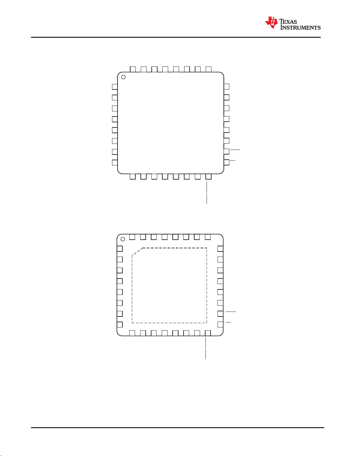
5 Pin Configuration and Functions...................................4
6 Specifications.................................................................. 6
6.1 Absolute Maximum Ratings ....................................... 6
6.2 ESD Ratings .............................................................. 6
6.3 Recommended Operating Conditions ........................7
6.4 Thermal Information ...................................................7
6.5 Electrical Characteristics ............................................9
6.6 Timing Requirements ............................................... 11
6.7 Switching Characteristics ......................................... 11
6.8 Timing Diagrams....................................................... 12
6.9 Typical Characteristics.............................................. 14
7 Parameter Measurement Information.......................... 19
7.1 Noise Measurements................................................ 19
8 Detailed Description......................................................20
8.1 Overview................................................................... 20
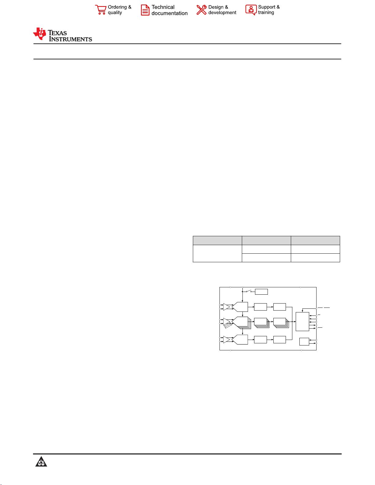
8.2 Functional Block Diagram......................................... 20
8.3 Feature Description...................................................21
8.4 Device Functional Modes..........................................32
8.5 Programming............................................................ 38
8.6 Registers...................................................................48
9 Application and Implementation.................................. 82
9.1 Application Information............................................. 82
9.2 Typical Application.................................................... 89
10 Power Supply Recommendations..............................96
10.1 CAP Pin Behavior................................................... 96
10.2 Power-Supply Sequencing......................................96
10.3 Power-Supply Decoupling.......................................96
11 Layout........................................................................... 97
11.1 Layout Guidelines................................................... 97
11.2 Layout Example...................................................... 98
12 Device and Documentation Support..........................99
12.1 Documentation Support.......................................... 99
12.2 接收文档更新通知................................................... 99
12.3 支持资源..................................................................99
12.4 Trademarks............................................................. 99
12.5 静电放电警告.......................................................... 99
12.6 术语表..................................................................... 99
13 Mechanical, Packaging, and Orderable
Information.................................................................... 99
4 Revision History
注:以前版本的页码可能与当前版本的页码不同
Changes from Revision * (February 2020) to Revision A (February 2021) Page
•
更新了整个文档中的表格、图和交叉参考的编号格式
........................................................................................ 1
• 将 WQFN 封装从预发布更改为正在供货............................................................................................................ 1
• 将
低功耗
要点的值从 5.0mW 更改为 4.9mW .....................................................................................................1
• 向
应用
部分添加了
保护继电器
和
电能质量监测仪
............................................................................................. 1
• 将首页上的 WQFN 封装从预发布更改为正在供货.............................................................................................. 1
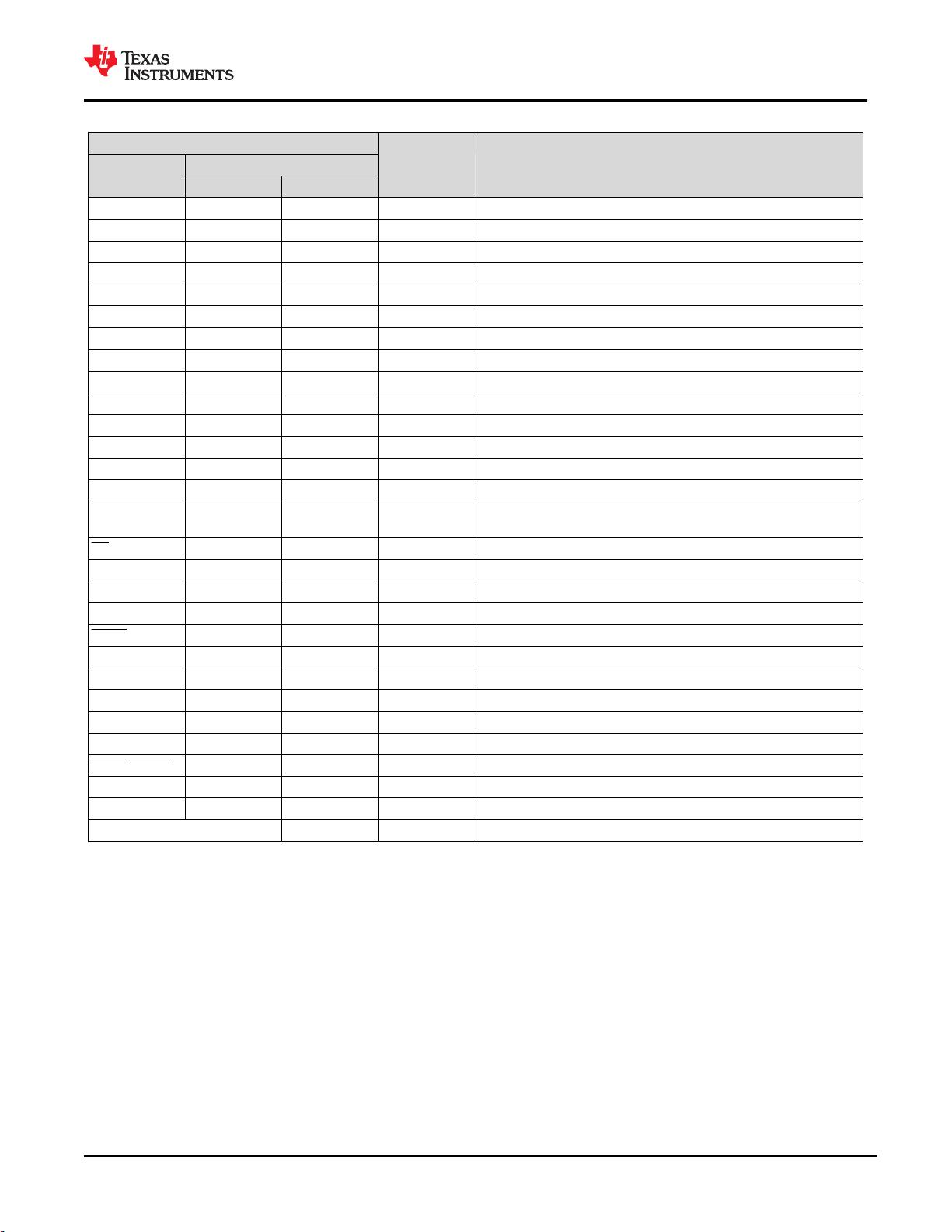
• Removed capacitor recommendation for REFIN pin in Pin Functions table ......................................................4
• Corrected analog input pin numbering in Pin Functions table ........................................................................... 4
• Added thermal pad to pinout diagram ................................................................................................................4
• Added Differential input voltage range using external reference ....................................................................... 7
• Added long-term reference and gain error drift in WQFN package in Electrical Characteristics table............... 9
• Added typical value for long term reference and gain error drift in WQFN package.......................................... 9
• Changed t
su(SY)
parameter description in Timing Requirements table .............................................................11
• Changed SPI Timing Diagram and SYNC/RESET Timing Requirements figures............................................ 12
• Added typical characteristics plots....................................................................................................................14
• Removed recommendation for decoupling capacitor when using internal reference....................................... 22
• Changed Clocking and Power Modes section, added internal oscillator option............................................... 23
• Changed description of modulator frequency and added f
MOD
equation in
ΔΣ
Modulator section.................23
• Changed Digital Filter section...........................................................................................................................23
• Changed Digital Filter Implementation title and section ...................................................................................24
• Updated description of the test signal derived from the internal reference ......................................................27
• Changed communication cyclic redundancy check (CRC) seed value............................................................ 30
• Added DRDY transitions in Power-Up and Reset section................................................................................ 32
• Moved Fast Startup Behavior section to Device Functional Modes section, and changed values for wait time
delays in text and figures.................................................................................................................................. 33
ADS131M06
ZHCSKW6A – FEBRUARY 2020 – REVISED FEBRUARY 2021
www.ti.com.cn
2 Submit Document Feedback
Copyright © 2021 Texas Instruments Incorporated
Product Folder Links: ADS131M06
• Added global-chop mode block diagram, global-chop mode conversion timing diagram, and 方程式 9 ......... 34
• Changed Standby Mode section ......................................................................................................................35
• Deleted comments about MOSI, MISO, slave, and master.............................................................................. 38
• Added description for new conversions when reading data in the Data Ready (DRDY) section......................38
• Added second paragraph to SPI Communication Frames section .................................................................. 39
• Changed Register Map table............................................................................................................................ 48
• Changed description sentence for each register section..................................................................................48
• Added pullup resistor option for DRDY in the Unused Inputs and Outputs section..........................................82
• Changed root cause description in Troubleshooting section ........................................................................... 88
• Changed discussion of burden resistor in Current Measurement Front-End section ...................................... 91
• Added ADC energy metrology library software to Related Documents ........................................................... 99
www.ti.com.cn
ADS131M06
ZHCSKW6A – FEBRUARY 2020 – REVISED FEBRUARY 2021
Copyright © 2021 Texas Instruments Incorporated
Submit Document Feedback
3
Product Folder Links: ADS131M06
5 Pin Configuration and Functions
31 30 29 28
10 11 12 13
4
3
2
1
18
19
20
21
AIN2P
AIN2N
AIN3N
AIN3P
AIN0P
CAP
XTAL1/CLKIN
AGND
DIN
XTAL2
AIN1N
AIN0N
17
DOUT
9
32
AIN1P
5
AIN4P
8
7
6
AIN4N
AIN5N
AIN5P
14 15 16
22
23
24
27 26 25
AVDD
REFIN
DVDD
NC
DRDY
SCLK
CS
DGND
AGND
SYNC/RESET
NC
NC
NC
NC
图 5-1. PBS Package, 32-Pin TQFP, Top View
31 30 29 28
10 11 12 13
4
3
2
1
18
19
20
21
AIN2P
AIN2N
AIN3N
AIN3P
NC
SYNC/RESET
AIN0P
CAP
XTAL1/CLKIN
AGND
DIN
XTAL2
AIN1N
AIN0N
NC
17
DOUT
9
NC
32
AIN1P
5
AIN4P
8
7
6
AIN4N
AIN5N
AIN5P
14 15 16
22
23
24
27 26 25
AVDD
REFIN
NC
DVDD
NC
DRDY
SCLK
CS
DGND
AGND
Exposed Thermal Pad
on Underside
Connect to AGND
图 5-2. RSN Package, 32-Pin WQFN, Top View
ADS131M06
ZHCSKW6A – FEBRUARY 2020 – REVISED FEBRUARY 2021
www.ti.com.cn
4 Submit Document Feedback
Copyright © 2021 Texas Instruments Incorporated
Product Folder Links: ADS131M06
表 5-1. Pin Functions
PIN
I/O DESCRIPTION
(1)
NAME
NO.
WQFN TQFP
AGND 13, 28 13, 28 Supply Analog ground
AIN0N 30 30 Analog input Negative analog input 0
AIN0P 29 29 Analog input Positive analog input 0
AIN1N 31 31 Analog input Negative analog input 1
AIN1P 32 32 Analog input Positive analog input 1
AIN2N 2 2 Analog input Negative analog input 2
AIN2P 1 1 Analog input Positive analog input 2
AIN3N 3 3 Analog input Negative analog input 3
AIN3P 4 4 Analog input Positive analog input 3
AIN4N 6 6 Analog input Negative analog input 4
AIN4P 5 5 Analog input Positive analog input 4
AIN5N 7 7 Analog input Negative analog input 5
AIN5P 8 8 Analog input Positive analog input 5
AVDD 15 15 Supply Analog supply. Connect a 1-µF capacitor to AGND.
CAP 24 24 Analog output
Digital low-dropout (LDO) regulator output.
Connect a 220-nF capacitor to DGND.
CS 17 17 Digital input Chip select; active low
DGND 25 25 Supply Digital ground
DIN 21 21 Digital input Serial data input
DOUT 20 20 Digital output Serial data output
DRDY 18 18 Digital output Data ready; active low
DVDD 26 26 Supply Digital I/O supply. Connect a 1-µF capacitor to DGND.
NC 9-12 9-12
—
Leave unconnected
NC 27 27
—
Leave unconnected or connect to AGND
REFIN 14 14 Analog input External reference voltage input.
(2)
SCLK 19 19 Digital input Serial data clock
SYNC/RESET 16 16 Digital input Conversion synchronization or system reset; active low
XTAL1/CLKIN 23 23 Digital input Master clock input, or crystal oscillator input
XTAL2 22 22 Digital output Crystal oscillator excitation
(3)
Thermal pad
— —
Thermal pad; connect to AGND
(1) See the Unused Inputs and Outputs section for details on how to connect unused pins.
(2) Do not place any capacitance on REFIN if the current-detect mode is used.
(3) See the Clocking and Power Modes section for more information regarding synchronization and how to implement the clocking
scheme for optimized device performance.
www.ti.com.cn
ADS131M06
ZHCSKW6A – FEBRUARY 2020 – REVISED FEBRUARY 2021
Copyright © 2021 Texas Instruments Incorporated
Submit Document Feedback
5
Product Folder Links: ADS131M06
剩余108页未读,继续阅读
资源评论
不觉明了
- 粉丝: 3118
- 资源: 5348
上传资源 快速赚钱
- 我的内容管理 展开
- 我的资源 快来上传第一个资源
- 我的收益 登录查看自己的收益
- 我的积分 登录查看自己的积分
- 我的C币 登录后查看C币余额
- 我的收藏
- 我的下载
- 下载帮助
最新资源
- ### 1、项目介绍 本项目Scrapy进行数据爬取,并使用Django框架+PyEcharts实现可视化大屏 效果如下:
- # 微信小程序-健康菜谱 基于微信小程序的一个查找检索菜谱的应用 ### 效果 !动态图(./res/gif/demo
- zabbix-get命令包资源
- 毕业设计,基于PyQt5实现的可视化界面的Python车牌自动识别系统源码
- 26-朴素贝叶斯分类.rar
- 没有安Matlab 也可以 生成FIR抽头系数工具.py
- python烟花代码.rar
- 实验目的: 1.构建基于verilog语言的组合逻辑电路和时序逻辑电路; 2.掌握verilog语言的电路设计技巧 3.完成如
- 扩展卡尔曼滤波matlab仿真
- 3_base.apk.1
资源上传下载、课程学习等过程中有任何疑问或建议,欢迎提出宝贵意见哦~我们会及时处理!
点击此处反馈
安全验证
文档复制为VIP权益,开通VIP直接复制
信息提交成功