没有合适的资源?快使用搜索试试~ 我知道了~
TI-ISO5852S.pdf
需积分: 5 0 下载量 198 浏览量
2022-11-11
23:54:07
上传
评论 5
收藏 2MB PDF 举报
温馨提示
试读
44页
TI-ISO5852S.pdf
资源详情
资源评论
GND1 V
EE2
RST
RDY
FLT
IN+
IN±
V
CC1
V
CC2
DESAT
GND2
OUTH
OUTL
CLAMP
V
CC1
V
CC1
UVLO1
Mute
Decoder
Q S
RQ
V
CC1
V
CC1
Gate Drive
and
Encoder
Logic
UVLO2
2 V
9 V
500 µA
STO
V
CC2
Ready
Fault
Copyright © 2016, Texas Instruments Incorporated
Product
Folder
Order
Now
Technical
Documents
Tools &
Software
Support &
Community
An IMPORTANT NOTICE at the end of this data sheet addresses availability, warranty, changes, use in safety-critical applications,
intellectual property matters and other important disclaimers. PRODUCTION DATA.
English Data Sheet: SLLSEQ0
ISO5852S
ZHCSE44B –AUGUST 2015–REVISED JANUARY 2017
ISO5852S 具具有有分分离离输输出出和和有有源源保保护护功功能能的的高高 CMTI 2.5A 和和 5A 增增强强型型隔隔
离离式式 IGBT、、MOSFET 栅栅极极
驱驱动动器器
1
1 特特性性
1
• V
CM
= 1500V 时的最低共模瞬态抗扰度 (CMTI) 为
100kV/μs
• 分离输出,可提供 2.5A 峰值拉电流和 5A 峰值灌电
流
• 短暂传播延迟:76ns(典型值),
110ns(最大值)
• 2A 有源米勒钳位
• 输出短路钳位
• 短路期间的软关断 (STO)
• 在检测到去饱和故障时通过 FLT 发出故障报警并通
过 RST 复位
• 具有就绪 (RDY) 引脚指示的输入和输出欠压锁定
(UVLO)
• 有源输出下拉特性,在低电源或输入悬空的情况下
默认输出低电平
• 2.25V 至 5.5V 输入电源电压
• 15V 至 30V 输出驱动器电源电压
• 互补金属氧化物半导体 (CMOS) 兼容输入
• 抑制短于 20ns 的输入脉冲和瞬态噪声
• 工作环境温度范围:–40°C 至 +125°C
• 可承受的浪涌隔离电压达 12800V
PK
”
• 安全相关认证:
– 符合 DIN V VDE V 0884-10 (VDE V 0884-
10):2006-12 标准的 8000 V
PK
V
IOTM
和 2121
V
PK
V
IORM
增强型隔离
– 符合 UL 1577 标准且长达 1 分钟的 5700 V
RMS
隔离
– CSA 组件验收通知 5A,IEC 60950-1 和 IEC
60601-1 终端设备标准
– 符合 EN 61010-1 和 EN 60950-1 标准的 TUV
认证
– GB4943.1-2011 CQC 认证
2 应应用用
• 隔离式绝缘栅双极型晶体管 (IGBT) 和金属氧化物
半导体场效应晶体管 (MOSFET) 驱动器:
– 工业电机控制驱动
– 工业电源
– 太阳能逆变器
– HEV 和 EV 电源模块
– 感应加热
3 说说明明
ISO5852S 器件是一款用于 IGBT 和 MOSFET 的 5.7
kV
RMS
增强型隔离栅极驱动器,具有分离输出(OUTH
和 OUTL)以及 2.5A 的拉电流能力和 5A 的灌电流能
力。输入端由 2.25V 至 5.5V 的单电源供电运行。输出
侧支持的电源电压范围为 15V 至 30V。两路互补
CMOS 输入控制栅极驱动器输出状态。76ns 的短暂传
播时间保证了对于输出级的精确控制。
内置的去饱和 (DESAT) 故障检测功能可识别 IGBT 何
时处于过流状态。检测到 DESAT 时,静音逻辑会立即
阻断隔离器输出,并启动软关断过程以禁用 OUTH 引
脚并将 OUTL 引脚拉至低电平持续 2μs。当 OUTL 引
脚达到 2V 时(相对于最大负电源电势 V
EE2
),栅极
驱动器会被“硬”拉至 V
EE2
电势,从而立即将 IGBT 关
断。
器器件件信信息息
(1)
器器件件型型号号 封封装装 封封装装尺尺寸寸((标标称称值值))
ISO5852S SOIC (16) 10.30mm x 7.50mm
(1) 要了解所有可用封装,请见数据表末尾的可订购产品附录。
功功能能框框图图
2
ISO5852S
ZHCSE44B –AUGUST 2015–REVISED JANUARY 2017
www.ti.com.cn
版权 © 2015–2017, Texas Instruments Incorporated
目目录录
1 特特性性.......................................................................... 1
2 应应用用.......................................................................... 1
3 说说明明.......................................................................... 1
4 修修订订历历史史记记录录 ........................................................... 2
5 说说明明 ((续续)).............................................................. 3
6 Pin Configuration and Function........................... 3
7 Specifications......................................................... 4
7.1 Absolute Maximum Ratings ...................................... 4
7.2 ESD Ratings.............................................................. 4
7.3 Recommended Operating Conditions....................... 4
7.4 Thermal Information.................................................. 5
7.5 Power Ratings........................................................... 5
7.6 Insulation Specifications............................................ 6
7.7 Safety-Related Certifications..................................... 7
7.8 Safety Limiting Values .............................................. 7
7.9 Electrical Characteristics........................................... 8
7.10 Switching Characteristics........................................ 9
7.11 Insulation Characteristics Curves ......................... 10
7.12 Typical Characteristics.......................................... 11
8 Parameter Measurement Information ................ 18
9 Detailed Description............................................ 20
9.1 Overview ................................................................. 20
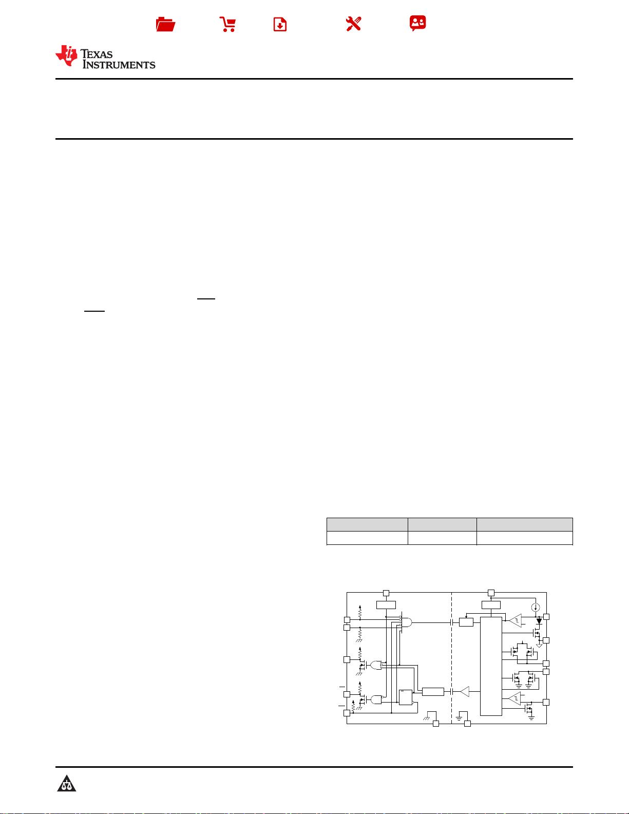
9.2 Functional Block Diagram ....................................... 20
9.3 Feature Description................................................. 21
9.4 Device Functional Modes........................................ 22
10 Application and Implementation........................ 23
10.1 Application Information.......................................... 23
10.2 Typical Applications .............................................. 23
11 Power Supply Recommendations ..................... 31
12 Layout................................................................... 31
12.1 Layout Guidelines ................................................. 31
12.2 PCB Material......................................................... 31
12.3 Layout Example .................................................... 31
13 器器件件和和文文档档支支持持 ..................................................... 32
13.1 文档支持................................................................ 32
13.2 接收文档更新通知 ................................................. 32
13.3 社区资源................................................................ 32
13.4 商标 ....................................................................... 32
13.5 静电放电警告......................................................... 32
13.6 Glossary................................................................ 32
14 机机械械、、封封装装和和可可订订购购信信息息....................................... 33
4 修修订订历历史史记记录录
注:之前版本的页码可能与当前版本有所不同。
Changes from Revision A (September 2015) to Revision B Page
• 已将特性“浪涌抗扰度高达 12800V
PK
(根据 IEC 61000-4-5)”更改为“可承受的浪涌隔离电压达 12800V
PK
.......................... 1
• Changed the minimum external tracking (creepage) parameter to the external creepage parameter .................................. 6
• Changed the input-to-output test voltage parameter to the apparent charge parameter....................................................... 6
• Added the climatic category to the Insulation Specifications table......................................................................................... 6
• Changed the CSA status from planned to certified ................................................................................................................ 7
• Added text ", but connecting CLAMP output of the gate driver to the IGBT gate is also not an issue." to Supply and
Active Miller Clamp............................................................................................................................................................... 21
• Changed the second paragraph of the Typical Applications................................................................................................ 23
• Added text "and RST input signal" to the Design Requirements ......................................................................................... 24
Changes from Original (July 2015) to Revision A Page
• 已将
特性
:“共模瞬态抗扰度的最小值为 100kV/μs..”移至列表顶部......................................................................................... 1
• 已更改 数据表标题中的“
有源安全 特性
”至“
有源保护 功能
”..................................................................................................... 1
• 已从单页产品预览更改为完整数据表。................................................................................................................................... 1
• 已将说明部分中的文本“3V 至 5.5V 单电源”更改至“2.25V
至
5.5V
单电源
” ............................................................................ 1
• 已将说明部分中的文本“IGBT 处于过载状态”更改至“IGBT
处于过流状态
” .............................................................................. 1
• 已将
中的文本由
“
并降低
OUTL
的电压持续
2μs
以上
”
更改为
“
并将
OUTL
拉至低电平持续
2μs”
说明
...................................... 1
• 更改了
功能框图
,在引脚 OUTL 上添加了 STO...................................................................................................................... 1
• 已更改
的第
3
段说明
............................................................................................................................................................... 3
• Changed the minimum air gap (clearance) parameter to the external clearance parameter................................................. 6
• 已更改
静电放电注意事项
..................................................................................................................................................... 32
1V
EE2
16 GND1
2DESAT 15 V
CC1
3GND2 14 RST
4OUTH 13 FLT
5 V
CC2
12 RDY
6OUTL 11 IN±
7CLAMP 10 IN+
8V
EE2
9 GND1
Not to scale
3
ISO5852S
www.ti.com.cn
ZHCSE44B –AUGUST 2015–REVISED JANUARY 2017
Copyright © 2015–2017, Texas Instruments Incorporated
5 说说明明 ((续续))
当发生去饱和故障时,器件会通过隔离隔栅发送故障信号,以将输入端的 FLT 输出拉为低电平并阻断隔离器的输
入。静音逻辑在软关断期间激活。FLT 的输出状态将被锁存,并只能在 RDY 引脚变为高电平后通过 RST 输入上的
低电平有效脉冲复位。
如果在由双极输出电源供电的正常运行期间关断 IGBT,输出电压会被硬钳位为 V
EE2
。如果输出电源为单极,那么
可采用有源米勒钳位,这种钳位会在一条低阻抗路径上灌入米勒电流,从而防止 IGBT 在高电压瞬态状态下发生动
态导通。
栅极驱动器是否准备就绪待运行由两个欠压锁定电路控制,这两个电路会监视输入端和输出端的电源。如果任意一
端电源不足,RDY 输出会变为低电平,否则该输出为高电平。
ISO5852S 采用 16 引脚小外形尺寸集成电路 (SOIC) 封装. 此器件的额定工作环境温度范围为 -40°C 至 +125°C。
6 Pin Configuration and Function
DW Package
16-Pin SOIC
Top View
Pin Functions
PIN
I/O DESCRIPTION
NAME NO.
CLAMP 7 O Miller clamp output
DESAT 2 I Desaturation voltage input
FLT 13 O Fault output, active-low during DESAT condition
GND1
9
— Input ground
16
GND2 3 — Gate drive common. Connect to IGBT emitter.
IN+ 10 I Non-inverting gate drive voltage control input
IN– 11 I Inverting gate drive voltage control input
OUTH 4 O Positive gate drive voltage output
OUTL 6 O Negative gate drive voltage output
RDY 12 O Power-good output, active high when both supplies are good.
RST 14 I Reset input, apply a low pulse to reset fault latch.
V
CC1
15 — Positive input supply (2.25-V to 5.5-V)
V
CC2
5 — Most positive output supply potential.
V
EE2
1
— Output negative supply. Connect to GND2 for unipolar supply application.
8
4
ISO5852S
ZHCSE44B –AUGUST 2015–REVISED JANUARY 2017
www.ti.com.cn
Copyright © 2015–2017, Texas Instruments Incorporated
(1) Stresses beyond those listed under Absolute Maximum Ratings may cause permanent damage to the device. These are stress ratings
only, which do not imply functional operation of the device at these or any other conditions beyond those indicated under Recommended
Operating Conditions. Exposure to absolute-maximum-rated conditions for extended periods may affect device reliability.
7 Specifications
7.1 Absolute Maximum Ratings
Over operating free-air temperature range (unless otherwise noted)
(1)
MIN MAX UNIT
V
CC1
Supply-voltage input side GND1 – 0.3 6 V
V
CC2
Positive supply-voltage output side (V
CC2
– GND2) –0.3 35 V
V
EE2
Negative supply-voltage output side (V
EE2
– GND2) –17.5 0.3 V
V
(SUP2)
Total-supply output voltage (V
CC2
– V
EE2
) –0.3 35 V
V
(OUTH)
Positive gate-driver output voltage V
EE2
– 0.3 V
CC2
+ 0.3 V
V
(OUTL)
Negative gate-driver output voltage V
EE2
– 0.3 V
CC2
+ 0.3 V
I
(OUTH)
Gate-driver high output current
Maximum pulse width = 10 μs, Maximum
duty cycle = 0.2%)
2.7 A
I
(OUTL)
Gate-driver low output current
Maximum pulse width = 10 μs, Maximum
duty cycle = 0.2%)
5.5 A
V
(LIP)
Voltage at IN+, IN–,FLT, RDY, RST GND1 – 0.3 V
CC1
+ 0.3 V
I
(LOP)
Output current of FLT, RDY 10 mA
V
(DESAT)
Voltage at DESAT GND2 – 0.3 V
CC2
+ 0.3 V
V
(CLAMP)
Clamp voltage V
EE2
– 0.3 V
CC2
+ 0.3 V
T
J
Junction temperature –40 150 °C
T
STG
Storage temperature –65 150 °C
(1) JEDEC document JEP155 states that 500-V HBM allows safe manufacturing with a standard ESD control process.
(2) JEDEC document JEP157 states that 250-V CDM allows safe manufacturing with a standard ESD control process.
7.2 ESD Ratings
VALUE UNIT
V
(ESD)
Electrostatic
discharge
Human body model (HBM), per ANSI/ESDA/JEDEC JS-001
(1)
±4000
V
Charged-device model (CDM), per JEDEC specification JESD22-C101
(2)
±1500
7.3 Recommended Operating Conditions
over operating free-air temperature range (unless otherwise noted)
MIN NOM MAX UNIT
V
CC1
Supply-voltage input side 2.25 5.5 V
V
CC2
Positive supply-voltage output side (V
CC2
– GND2) 15 30 V
V
(EE2)
Negative supply-voltage output side (V
EE2
– GND2) –15 0 V
V
(SUP2)
Total supply-voltage output side (V
CC2
– V
EE2
) 15 30 V
V
(IH)
High-level input voltage (IN+, IN–, RST) 0.7 × V
CC1
V
CC1
V
V
(IL)
Low-level input voltage (IN+, IN–, RST) 0 0.3 × V
CC1
V
t
UI
Pulse width at IN+, IN– for full output (C
LOAD
= 1 nF) 40 ns
t
RST
Pulse width at RST for resetting fault latch 800 ns
T
A
Ambient temperature –40 125 °C
5
ISO5852S
www.ti.com.cn
ZHCSE44B –AUGUST 2015–REVISED JANUARY 2017
Copyright © 2015–2017, Texas Instruments Incorporated
(1) For more information about traditional and new thermal metrics, see the Semiconductor and IC Package Thermal Metrics application
report.
7.4 Thermal Information
THERMAL METRIC
(1)
ISO5852S
UNITDW (SOIC)
16 PINS
R
θJA
Junction-to-ambient thermal resistance 99.6 °C/W
R
θJC(top)
Junction-to-case (top) thermal resistance 48.5 °C/W
R
θJB
Junction-to-board thermal resistance 56.5 °C/W
ψ
JT
Junction-to-top characterization parameter 29.2 °C/W
ψ
JB
Junction-to-board characterization parameter 56.5 °C/W
7.5 Power Ratings
Full-chip power dissipation is derated 10.04 mW/°C beyond 25°C ambient temperature. At 125°C ambient temperature, a
maximum of 251 mW total power dissipation is allowed. Power dissipation can be optimized depending on ambient
temperature and board design, while ensuring that the junction temperature does not exceed 150 ° C.
PARAMETER TEST CONDITIONS MIN TYP MAX UNIT
P
D
Maximum power dissipation (both sides) V
CC1
= 5.5 V, V
CC2
= 30 V, T
A
= 25°C 1255 mW
P
ID
Maximum input power dissipation V
CC1
= 5.5 V, V
CC2
= 30 V, T
A
= 25°C 175 mW
P
OD
Maximum output power dissipation V
CC1
= 5.5 V, V
CC2
= 30 V, T
A
= 25°C 1080 mW
剩余43页未读,继续阅读
安全验证
文档复制为VIP权益,开通VIP直接复制
信息提交成功
评论0
最新资源