TI-ADS130E08.pdf
需积分: 18 29 浏览量
2022-12-04
20:47:23
上传
评论 4
收藏 1.58MB PDF 举报

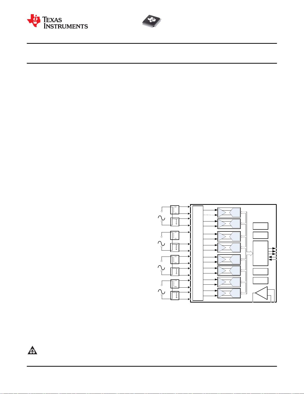
EMI
Filters
and
Input
MUX
Control
and
SPI Interface
Voltage
Reference
Oscillator
Fault
Detection
Test
Device
Current
Sensing
Line A
Voltage
Sensing
Channel 1
Channel 2
Channel 3
PGA
û
ADC
PGA
û
ADC
PGA
û
ADC
Current
Sensing
Voltage
Sensing
Current
Sensing
Voltage
Sensing
Current
Sensing
Voltage
Sensing
PGA
û
ADC
PGA
û
ADC
PGA
û
ADC
Channel 4
Channel 5
Channel 6
Channel 7
Channel 8
PGA
û
ADC
PGA
û
ADC
Line B
Line C
Line N
Op
Amp
ADS130E08
www.ti.com.cn
ZHCS975A –JULY 2012–REVISED SEPTEMBER 2012
用用于于计计量量应应用用的的低低成成本本、、8 通通道道、、集集成成模模拟拟前前端端
查查询询样样品品: ADS130E08
1
特特性性
说说明明
23
• 8 个个差差分分电电流流和和电电压压输输入入
ADS130E08 是一款多通道、同步采样、16 位、三角
• 8 个个低低噪噪声声可可编编程程增增益益放放大大器器 (PGA) 与与
积分 (ΔΣ) 模数转换器 (ADC),此转换器带有内置可编
8 个个高高分分辨辨率率模模数数转转换换器器 (ADC)
程增益放大器 (PGA),内部基准,和一个外部振荡器
• 超超过过 1.0 类类性性能能
接口。
• 共共模模抑抑制制比比 (CMRR):: –110 dB
• 串串扰扰::-105dB
此器件组装有工业仪表计量应用中的常用特性。 凭借
• 总总谐谐波波失失真真 (THD)::-108dB
其高度的集成性及出色的性能,ADS130E08 系列产品
• 功功率率::每每通通道道 750µW
能够在大幅缩小尺寸、降低功耗与整体成本的同时,创
• 数数据据速速率率::8 每每秒秒千千次次采采样样 (kSPS)
建可扩展工业电源系统。
• 可可编编程程增增益益((1,,2,,和和 8))
ADS130E08 每通道上提供一个灵活的输入多路复用
• 直直流流耦耦合合::
器,此多路复用器可独立连接至内部生成的信号来实现
– 双双电电源源::+3V 至至 +5V 或或者者
测试、温度、和故障检测。 ADS130E08 运行数据速
+1.8V 至至 +3.6V
率为 8kSPS。 故障检测可在器件内部执行,此器件使
– 双双极极电电源源::±2.5V
用由数模转换器 (DAC) 控制触发电平的集成比较器。
• 内内置置测测试试信信号号
• 故故障障检检测测比比较较器器
可在菊花链配置的高通道数量系统中串联多个器件。
• 四四个个通通用用输输入入输输出出 (GPIO) 引引脚脚
这些完整的模拟前端 (AFE) 解决方案采用 TQFP-64 封
• 内内部部和和外外部部基基准准
装,额定工业温度范围为 -40°C 至 +105°C。
• 灵灵活活的的省省电电模模式式::STBY((待待机机))模模式式
• 串串行行外外设设接接口口 (SPI)™ 数数据据接接口口
• 封封装装::薄薄型型四四方方扁扁平平封封装装 (TQFQ)-64 (PAG)
• 工工作作温温度度范范围围::
-40°C 至至 +105°C
应应用用范范围围
• 工工业业电电源源应应用用::
– 三三相相仪仪表表计计量量
– 工工业业应应用用
1
Please be aware that an important notice concerning availability, standard warranty, and use in critical applications of
Texas Instruments semiconductor products and disclaimers thereto appears at the end of this data sheet.
2串行外设接口 (SPI) is a trademark of Motorola.
3All other trademarks are the property of their respective owners.
PRODUCTION DATA information is current as of publication date.
Copyright © 2012, Texas Instruments Incorporated
Products conform to specifications per the terms of the Texas
Instruments standard warranty. Production processing does not English Data Sheet: SBAS574
necessarily include testing of all parameters.
剩余51页未读,继续阅读
资源评论


