TI-LMK61E08.pdf
需积分: 9 134 浏览量
2022-11-30
22:55:11
上传
评论 4
收藏 1.36MB PDF 举报

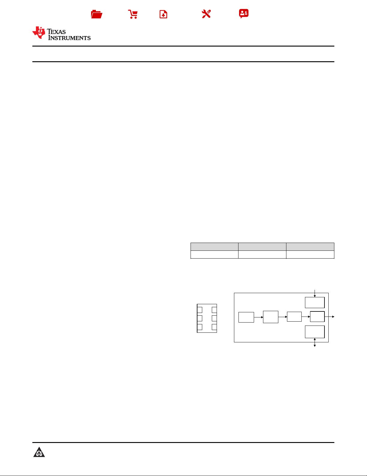
SCL OUTN
VDDSDA
GND OUTP
1 6
2 5
43
LMK61E0X
Ultra-high performance oscillator
PLL
Output
Divider
Output
Buffer
Power
Conditioning
Interface
I
2
C/EEPROM
Integrated
Oscillator
Copyright © 2016, Texas Instruments Incorporated
Product
Folder
Order
Now
Technical
Documents
Tools &
Software
Support &
Community
An IMPORTANT NOTICE at the end of this data sheet addresses availability, warranty, changes, use in safety-critical applications,
intellectual property matters and other important disclaimers. PRODUCTION DATA.
LMK61E08
SNAS805 –JUNE 2020
LMK61E08 Ultra-Low Jitter Programmable Oscillator With Internal EEPROM
1
1 Features
1
• Ultra-Low Noise, High Performance
– Jitter: 90-fs RMS Typical f
OUT
> 100 MHz on
LMK61E08
– PSRR: –70 dBc, Robust Supply Noise
Immunity on LMK61E08
• Flexible Output Format on LMK61E08
– LVPECL up to 1 GHz
– LVDS up to 900 MHz
– HCSL up to 400 MHz
• Total Frequency Tolerance of ±25 ppm
• System Level Features
– Glitch-Less Frequency Margining: Up to ±1000
ppm From Nominal
– Internal EEPROM: User Configurable Start-Up
Settings
• Other Features
– Device Control: Fast Mode I
2
C up to 1000 kHz
– 3.3-V Operating Voltage
– Industrial Temperature Range (–40ºC to
+85ºC)
– 7-mm × 5-mm 6-Pin Package
• Default Frequency:
– 70.656 MHz
2 Applications
• High-Performance Replacement for Crystal, SAW,
or Silicon-Based Oscillators
• Switches, Routers, Network Line Cards, Base
Band Units (BBU), Servers, Storage/SAN
• Test and Measurement
• Medical Imaging
• FPGA, Processor Attach
• xDSL, Broadcast Video
3 Description
The LMK61E08 family of ultra-low jitter PLLatinum™
programmable oscillators uses fractional-N frequency
synthesizers with integrated VCOs to generate
commonly used reference clocks. The output on
LMK61E08 can be configured as LVPECL, LVDS, or
HCSL. The device features self-start-up from on-chip
EEPROM to generate a factory-programmed default
output frequency, or the device registers and
EEPROM settings are fully programmable in-system
through an I
2
C serial interface. The device provides
fine and coarse frequency margining control through
an I
2
C serial interface, making it a digitally-controlled
oscillator (DCXO).
The PLL feedback divider can be updated to adjust
the output frequency without spikes or glitches in
steps of <1ppb using a PFD of 12.5 MHz (R
divider=4, doubler disabled) for compatibility with
xDSL requirements, or in steps of <5.2 ppb using a
PFD of 100 MHz (R divider=1, doubler enabled) for
compatibility with broadcast video requirements. The
frequency margining features also facilitate system
design verification tests (DVT), such as standards
compliance and system timing margin testing.
Device Information
(1)
PART NUMBER PACKAGE BODY SIZE (NOM)
LMK61E08 QFM (6) 7.00 mm × 5.00 mm
(1) For all available packages, see the orderable addendum at
the end of the data sheet.
Pinout and Simplified Block Diagram

剩余53页未读,继续阅读


评论0
最新资源