没有合适的资源?快使用搜索试试~ 我知道了~
TI-UCD9081.pdf
需积分: 9 0 下载量 87 浏览量
2022-11-16
23:08:41
上传
评论 5
收藏 2.41MB PDF 举报
温馨提示
![preview](https://dl-preview.csdnimg.cn/87044856/0001-8adf5aa688d6c4adba23ddbf10d6d1a7_thumbnail.jpeg)
![preview-icon](https://csdnimg.cn/release/downloadcmsfe/public/img/scale.ab9e0183.png)
试读
38页
TI-UCD9081.pdf
资源推荐
资源详情
资源评论
![](https://csdnimg.cn/release/download_crawler_static/87044856/bg1.jpg)
MON1
MON2
MON3
MON4
MON5
MON6
MON7
MON8
Oscillator
Status
Registers
10-bit
SAR ADC
I C
Engine
2
Power
Enables
EN1
EN2
EN3
EN4
EN5
EN6
EN7
EN8/GPO1
General-
Purpose
Outputs
GPO2
GPO3
GPO4
Config
Memory
Error Log
Flash
Memory
SCL SDA
Analog
Inputs
Sequencing
Engine
Copyright © 2016, Texas Instruments Incorporated
UCD 9081
EN[1:7]
SDA
SCL
VCC
VSS
MON [1:8]
A1
ROSC
RST
XIN
TEST
10 kW
100 kW
10 kW
10 kW
3.3V
3.3V 3.3V
3.3V
3.3V
3.3V
3.3V
0.01 Fm
1 Fm
A2
A3
A4
EN
EN
EN
V
OUT1
V
OUTX
V
OUT2
Slave I C
Address
2
To I C
2
Master Device
Digital
Outputs
EN8/
ADDR1/
GPO1
ADDR2/
GPO2
ADDR3/
GPO3
ADDR4/
GPO4
Power
Supply
1
Power
Supply
2
Power
Supply
X
Copyright © 2016, Texas Instruments Incorporated
Product
Folder
Sample &
Buy
Technical
Documents
Tools &
Software
Support &
Community
An IMPORTANT NOTICE at the end of this data sheet addresses availability, warranty, changes, use in safety-critical applications,
intellectual property matters and other important disclaimers. PRODUCTION DATA.
UCD9081
SLVS813C –JUNE 2008–REVISED NOVEMBER 2016
UCD9081 8-Channel Power Supply Sequencer and Monitor With Error Logging
1
1 Features
1
• Single Supply Voltage: 3.3 V
• Low Power Consumption: 3-mA Nominal Supply
Current
• Sequences and Monitors Eight Voltage Rails
• Rail Voltages Sampled With 3.2-mV Resolution
• Internal or External Voltage Reference
• Four Configurable Digital Outputs for Power-On-
Reset and Other Functions
• Configurable Digital Output Polarity
• Flexible Rail Sequencing Based on Timeline (ms),
Parent Rail Regulation Window, or Parent Rail
Achieving Defined Threshold
• Independent Under- and Overvoltage Thresholds
Per Rail
• Configurable Regulation Expiration Times Per Rail
• Flexible Alarm Processing: Ignore, Log Only,
Retry n Times, Retry Continuously, Sequence,
Parent Rail Can Shutdown Child Rails
• Alarm Conditions Logged With Timestamp: Under-
and Overvoltage Glitch, Sustained Under- and
Overvoltage, Rail Did Not Start
• On-Chip Flash for Storing User Data
• Error Logging to Flash for System Failure Analysis
• I
2
C™ Interface for Configuration and Monitoring
• Microsoft Windows™ GUI for Configuration and
Monitoring
Functional Block Diagram
2 Applications
• Telecommunications Switches
• Servers
• Networking Equipment
• Test Equipment
• Industrial
• Any System Requiring Sequencing of Multiple
Voltage Rails
3 Description
The UCD9081 power-supply sequencer controls the
enable sequence of up to eight independent voltage
rails and provides four general-purpose digital outputs
(GPO). The device operates from a 3.3-V supply,
provides 3.2-mV resolution of voltage rails, and
requires no external memory or clock. The UCD9081
monitors the voltage rails independently and has a
high degree of rail sequence and alarm response
options. The sequencing of rails can be based on
timed events or on timed events in conjunction with
other rails achieving regulation or a voltage threshold.
In addition, each rail is monitored for undervoltage
and overvoltage glitches and thresholds. Each rail the
UCD9081 monitors can be configured to shut down a
user-defined set of other rails and GPOs, and alarm
conditions are monitored on a per-rail basis.
Figure 20 shows the UCD9081 power-supply
sequencer in a typical application.
Device Information
(1)
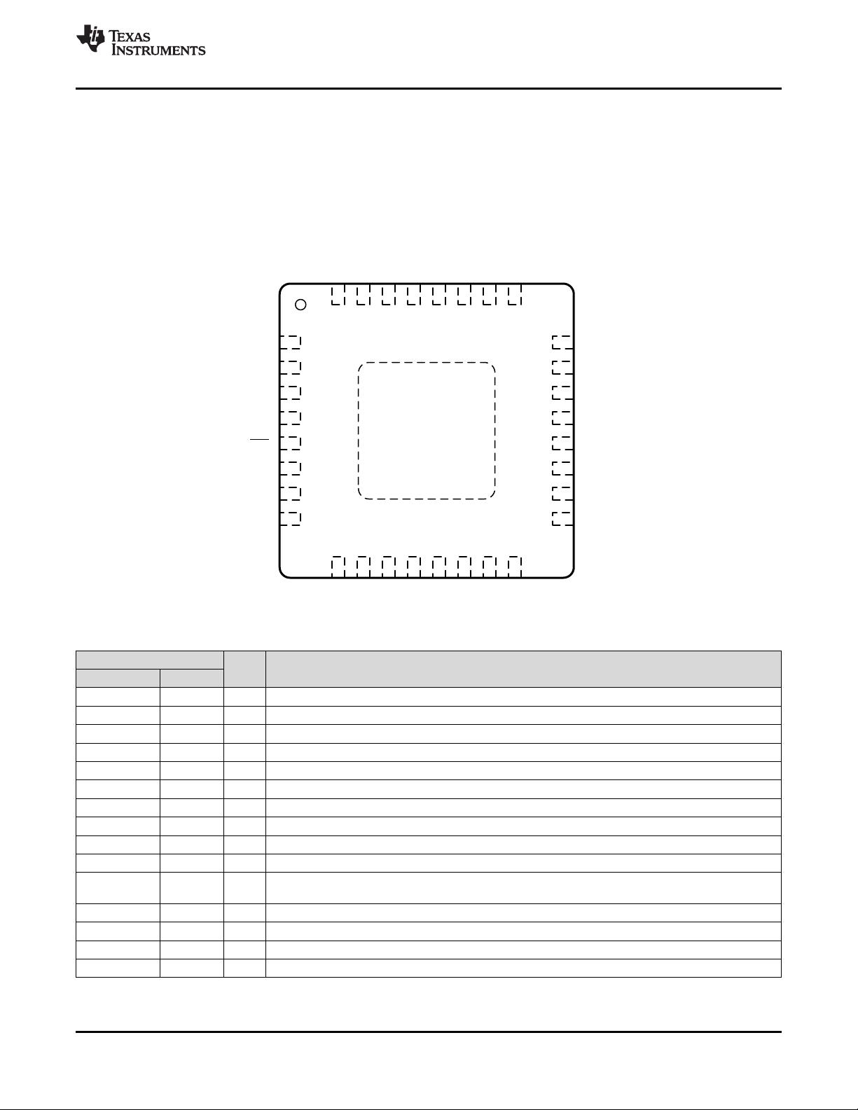
PART NUMBER PACKAGE BODY SIZE (NOM)
UCD9081 VQFN (32) 5.00 mm × 5.00 mm
(1) For all available packages, see the orderable addendum at
the end of the data sheet.
Typical Application Diagram
![](https://csdnimg.cn/release/download_crawler_static/87044856/bg2.jpg)
2
UCD9081
SLVS813C –JUNE 2008–REVISED NOVEMBER 2016
www.ti.com
Product Folder Links: UCD9081
Submit Documentation Feedback Copyright © 2008–2016, Texas Instruments Incorporated
Table of Contents
1 Features.................................................................. 1
2 Applications ........................................................... 1
3 Description ............................................................. 1
4 Revision History..................................................... 2
5 Pin Configuration and Functions......................... 3
6 Specifications......................................................... 5
6.1 Absolute Maximum Ratings ...................................... 5
6.2 Recommended Operating Conditions....................... 5
6.3 Thermal Information.................................................. 5
6.4 Electrical Characteristics........................................... 5
6.5 Timing Requirements: I
2
C Interface.......................... 6
6.6 Typical Characteristics.............................................. 7
7 Parameter Measurement Information .................. 8
8 Detailed Description .............................................. 9
8.1 Overview ................................................................... 9
8.2 Functional Block Diagram ......................................... 9
8.3 Feature Description................................................. 10
8.4 Device Functional Modes........................................ 11
8.5 Programming........................................................... 14
8.6 Register Maps......................................................... 18
9 Application and Implementation ........................ 24
9.1 Application Information............................................ 24
9.2 Typical Application .................................................. 25
10 Power Supply Recommendations ..................... 28
11 Layout................................................................... 28
11.1 Layout Guidelines ................................................. 28
11.2 Layout Example .................................................... 28
12 Device and Documentation Support ................. 29
12.1 Documentation Support ........................................ 29
12.2 Receiving Notification of Documentation Updates 29
12.3 Community Resources.......................................... 29
12.4 Trademarks........................................................... 29
12.5 Electrostatic Discharge Caution............................ 29
12.6 Glossary................................................................ 29
13 Mechanical, Packaging, and Orderable
Information ........................................................... 29
4 Revision History
NOTE: Page numbers for previous revisions may differ from page numbers in the current version.
Changes from Revision B (December 2010) to Revision C Page
• Added ESD Ratings table, Feature Description section, Device Functional Modes, Application and Implementation
section, Power Supply Recommendations section, Layout section, Device and Documentation Support section, and
Mechanical, Packaging, and Orderable Information section .................................................................................................. 1
• Deleted Ordering Information table; see POA at the end of the data sheet........................................................................... 1
• Added Thermal Information table ........................................................................................................................................... 5
• Moved Timing Parameters for I
2
C Interface table and I
2
C Timing diagram to Specifications................................................ 6
• Moved content in Monitoring the UCD9081 to Register Maps............................................................................................. 18
Changes from Revision A (September 2008) to Revision B Page
• Added Note 1 to the PIN FUNCTIONS table ......................................................................................................................... 3
• Added Note regarding state of enable and digital I/O pins when the device contains factory configuration ....................... 15
• Added a reference to the UCD9081 Programming Guide.................................................................................................... 16
Changes from Original (June 2008) to Revision A Page
• Changed the data sheet from Product Preview to Production; multiple changes throughout................................................ 1
• Changed first RAIL voltage equation From: × V
REF
To: × V
R+
............................................................................................. 19
• Changed second RAIL voltage equation From: × V
REF
To: × V
R+
....................................................................................... 19
![](https://csdnimg.cn/release/download_crawler_static/87044856/bg3.jpg)
32 ROSC9MON6
1VSS 24 EN2
31 NC10EN4
2NC 23 EN1
30 VCC 11EN3
3XIN 22 SCL
29 TEST12EN5
4NC 21 SDA
28 ADDR4/GPO413EN6
5RST 20 NC
27 ADDR3/GPO314EN7
6MON1 19 MON5
26 ADDR2/GPO215MON7
7MON2 18 MON4
25 EN8/ADDR1/GPO116MON8
8MON3 17 NC
Not to scale
PowerPAD
3
UCD9081
www.ti.com
SLVS813C –JUNE 2008–REVISED NOVEMBER 2016
Product Folder Links: UCD9081
Submit Documentation FeedbackCopyright © 2008–2016, Texas Instruments Incorporated
(1) Enable and GPIO pins are in high-impedance state when a device is received from factory and during the first configuration
programming done by customer.
5 Pin Configuration and Functions
RHB Package
32-Pin VQFN
Top View
Pin Functions
PIN
(1)
I/O DESCRIPTION
NAME NO.
ADDR2/GPO2 26 I/O I
2
C address select 2, general-purpose digital output 2
ADDR3/GPO3 27 I/O I
2
C address select 3, general-purpose digital output 3
ADDR4/GPO4 28 I/O I
2
C address select 4, general-purpose digital output 4
EN1 23 I/O Voltage rail 1 enable (digital output)
EN2 24 I/O Voltage rail 2 enable (digital output)
EN3 11 I/O Voltage rail 3 enable (digital output)
EN4 10 I/O Voltage rail 4 enable (digital output)
EN5 12 I/O Voltage rail 5 enable (digital output)
EN6 13 I/O Voltage rail 6 enable (digital output)
EN7 14 I/O Voltage rail 7 enable (digital output)
EN8/ADDR1/
GPO1
25 I/O Voltage rail 8 enable (digital output), I
2
C address select 1, general-purpose digital output 1
MON1 6 I Analog input for voltage rail 1
MON2 7 I Analog input for voltage rail 2
MON3 8 I Analog input for voltage rail 3
MON4 18 I Analog input for voltage rail 4
![](https://csdnimg.cn/release/download_crawler_static/87044856/bg4.jpg)
4
UCD9081
SLVS813C –JUNE 2008–REVISED NOVEMBER 2016
www.ti.com
Product Folder Links: UCD9081
Submit Documentation Feedback Copyright © 2008–2016, Texas Instruments Incorporated
Pin Functions (continued)
PIN
(1)
I/O DESCRIPTION
NAME NO.
MON5 19 I Analog input for voltage rail 5
MON6 9 I Analog input for voltage rail 6
MON7 15 I Analog input for voltage rail 7
MON8 16 I Analog input for voltage rail 8
NC 2 — Do not connect
NC
4, 17,
20, 31
— Recommended to connect to V
SS
, pin is not connected internally
ROSC 32 —
Internal oscillator frequency adjust. Must use 100-kΩ pullup to V
CC
for minimum drift and maximum
frequency when sampling voltage rails.
RST 5 I Reset input
SCL 22 I/O I
2
C clock. Must pull up to 3.3 V.
SDA 21 I/O I
2
C data. Must pull up to 3.3 V.
TEST 29 I Connect to V
SS
V
CC
30 — Supply voltage
V
SS
1 — Ground reference
XIN 3 — Connect to V
CC
PowerPAD™ — — Package pad. Recommended to connect to V
SS
.
![](https://csdnimg.cn/release/download_crawler_static/87044856/bg5.jpg)
5
UCD9081
www.ti.com
SLVS813C –JUNE 2008–REVISED NOVEMBER 2016
Product Folder Links: UCD9081
Submit Documentation FeedbackCopyright © 2008–2016, Texas Instruments Incorporated
(1) Stresses beyond those listed under Absolute Maximum Ratings may cause permanent damage to the device. These are stress ratings
only, which do not imply functional operation of the device at these or any other conditions beyond those indicated under Recommended
Operating Conditions. Exposure to absolute-maximum-rated conditions for extended periods may affect device reliability.
(2) All voltages referenced to V
SS
.
6 Specifications
6.1 Absolute Maximum Ratings
over operating free-air temperature range (unless otherwise noted)
(1)
MIN MAX UNIT
Voltage applied from V
CC
to V
SS
–0.3 4.1 V
Voltage applied to any pin
(2)
–0.3 V
CC
+ 0.3 V
ESD diode current at any device terminal ±2 mA
Storage temperature, T
stg
–40 85 °C
6.2 Recommended Operating Conditions
MIN NOM MAX UNIT
V
CC
Supply voltage during operation and configuration changes 3 3.3 3.6 V
T
A
Operating free-air temperature –40 85 °C
(1) For more information about traditional and new thermal metrics, see the Semiconductor and IC Package Thermal Metrics application
report.
6.3 Thermal Information
THERMAL METRIC
(1)
UCD9081
UNITRHB (VQFN)
32 PINS
R
θJA
Junction-to-ambient thermal resistance 32.1 °C/W
R
θJC(top)
Junction-to-case (top) thermal resistance 18.1 °C/W
R
θJB
Junction-to-board thermal resistance 6 °C/W
ψ
JT
Junction-to-top characterization parameter 0.2 °C/W
ψ
JB
Junction-to-board characterization parameter 5.9 °C/W
R
θJC(bot)
Junction-to-case (bottom) thermal resistance 1.2 °C/W
6.4 Electrical Characteristics
These specifications are over recommended ranges of supply voltage and operating free-air temperature (unless otherwise
noted)
PARAMETER TEST CONDITIONS MIN TYP MAX UNIT
SUPPLY CURRENT
I
S
Supply current into V
CC
T
A
= 25°C, excluding external current 3 4 mA
I
C
Supply current during configuration V
CC
= 3.6 V 3 7 mA
STANDARD INPUTS (RST, TEST)
V
IL
Low-level input voltage V
CC
= 3 V V
SS
V
SS
+ 0.6 V
V
IH
High-level input voltage V
CC
= 3 V 0.8 × V
CC
V
CC
V
SCHMITT TRIGGER INPUTS (SDA, SCL, EN[1...7], EN8/ADDR1, ADDR[2...4])
V
IT+
Positive-going input threshold voltage V
CC
= 3 V 1.5 1.9 V
V
IT–
Negative-going input threshold voltage V
CC
= 3 V 0.9 1.3 V
V
hys
Input voltage hysteresis V
CC
= 3 V, V
IT+
– V
IT–
0.5 1 V
I
lkg
High-impedance leakage current ±50 nA
ANALOG INPUTS (MONx, ROSC)
V
CC
Analog supply voltage V
SS
= 0 V 3 3.6 V
V
MON<1..8>
Analog input voltage
Internal voltage reference selected 0 2.5
V
External voltage reference selected
(V
CC
used as reference)
0 V
CC
剩余37页未读,继续阅读
资源评论
![avatar-default](https://csdnimg.cn/release/downloadcmsfe/public/img/lazyLogo2.1882d7f4.png)
![avatar](https://profile-avatar.csdnimg.cn/107303f5121d47e49d12d0a9ae68af10_weixin_54787054.jpg!1)
不觉明了
- 粉丝: 3236
- 资源: 5614
上传资源 快速赚钱
我的内容管理 展开
我的资源 快来上传第一个资源
我的收益
登录查看自己的收益我的积分 登录查看自己的积分
我的C币 登录后查看C币余额
我的收藏
我的下载
下载帮助
![voice](https://csdnimg.cn/release/downloadcmsfe/public/img/voice.245cc511.png)
![center-task](https://csdnimg.cn/release/downloadcmsfe/public/img/center-task.c2eda91a.png)
安全验证
文档复制为VIP权益,开通VIP直接复制
![dialog-icon](https://csdnimg.cn/release/downloadcmsfe/public/img/green-success.6a4acb44.png)