TI-UCD90124.pdf
需积分: 9 94 浏览量
2022-11-16
23:09:36
上传
评论 5
收藏 3.35MB PDF 举报

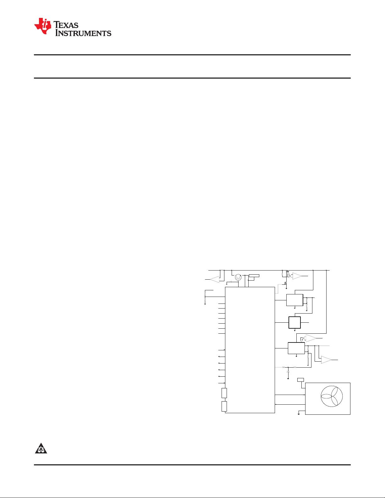
Vmarg
Closed Loop
Margining
UCD90124
VMON
GPIO
12V
V33FB
V33A
V33D
GPIO
3.3V OUT
VMON
1.8V OUT
3.3V_UCD
0.8V OUT
I0.8V
TEMP0.8V
VMON
VMON
VMON
VMON
I12V
TEMP12V
VMON
VMON
INA196
I12V
12V OUT
3.3V OUT
12V OUT
1.8V OUT
GPIO
GPIO
0.8V OUT
PWM
2MHz
INA196
I0.8V
WDI from main
processor
GPIO
WDO
GPIO
TEMP IC
TEMP0.8V
TEMP IC
TEMP12V
POWER_GOOD
GPIO
WARN_OC_0.8V_
OR_12V
GPIO
SYSTEM RESET
GPIO
OTHER
SEQUENCER DONE
(CASCADE INPUT)
GPIO
I2C/
PMBUS
JT
AG
/EN
DC-DC 1
VOUT
VFB
VIN
/EN
LDO1
VOUT
VIN
/EN
DC-DC 2
VOUT
VFB
VIN
V
4- wire Fan
12 V
4-
DC Fan
PWM
GPIO
Fan T
ach
25 kHz Fan PWM
12V
T
ACH
PWM
GND
5.1V
UCD90124
www.ti.com
SLVSA29B –NOVEMBER 2009–REVISED SEPTEMBER 2010
12-Rail Sequencer and System Health Monitor With Fan Control
Check for Samples: UCD90124
1
FEATURES
DESCRIPTION
2
• Monitor and Sequence 12 Voltage Rails
– All Rails Sampled Every 400 ms
The UCD90124 is a 12-rail PMBus/I
2
C addressable
power-supply sequencer and system-health
– 12-bit ADC With 2.5-V, 0.5% Internal V
REF
monitor. The device integrates a 12-bit ADC for
– Sequence Based on Time, Rail and Pin
monitoring up to 13 power-supply voltage, current, or
Dependencies
temperature inputs. Twenty-six GPIO pins can be
– Four Programmable Undervoltage and used for power supply enables, power-on reset
signals, external interrupts, cascading, or other
Overvoltage Thresholds per Monitor
system functions. Twelve of these pins offer PWM
• Fan Control and Monitoring
functionality. Using these pins, the UCD90124 offers
– Supports Four Fans With Five User-Defined
support for fan control, margining, and
Speed-vs-Temperature Setpoints
general-purpose PWM functions.
– Supports Two-, Three-, and Four-Wire Fans
Fan-control signals can be sent using PMBus
• Nonvolatile Error and Peak-Value Logging per
commands or generated from one of two built-in
Monitor (up to 10 Fault Detail Entries)
fan-control algorithms. PWM outputs combined with
temperature and fan-speed measurements provide a
• Closed-Loop Margining for 10 Rails
complete fan-control solution for up to four
– Margin Output Adjusts Rail Voltage to
independent fans.
Match User-Defined Margin Thresholds
The TI Fusion Digital Power™ designer software is
• Programmable Watchdog Timer and System
provided for device configuration. This PC-based
Reset
graphical user interface (GUI) offers an intuitive
• Flexible Digital I/O Configuration
interface for configuring, storing, and monitoring all
system operating parameters.
• Multiphase PWM Clock Generator
– Clock Frequencies From 15.259 kHz to 125
MHz
– Capability to Configure Independent Clock
Outputs for Synchronizing Switch-Mode
Power Supplies
• Internal Temperature Sensor
• JTAG and I
2
C/SMBus/ PMBus™ Interfaces
APPLICATIONS
• Industrial / ATE
• Telecommunications and Networking
Equipment
• Servers and Storage Systems
• Embedded Computing
• Any System Requiring Sequencing and
Monitoring of Multiple Power Rails
1
Please be aware that an important notice concerning availability, standard warranty, and use in critical applications of Texas
Instruments semiconductor products and disclaimers thereto appears at the end of this data sheet.
2PMBus, Fusion Digital Power are trademarks of Texas Instruments.
PRODUCTION DATA information is current as of publication date.
Copyright © 2009–2010, Texas Instruments Incorporated
Products conform to specifications per the terms of the Texas
Instruments standard warranty. Production processing does not
necessarily include testing of all parameters.

剩余48页未读,继续阅读
资源评论


