TI-TL598.pdf
需积分: 9 15 浏览量
2022-10-26
23:32:38
上传
评论 5
收藏 916KB PDF 举报

SLVS053D − FEBRUARY 1988 − REVISED NOVEMBER 2003
1
POST OFFICE BOX 655303 • DALLAS, TEXAS 75265
D Complete PWM Power-Control Function
D Totem-Pole Outputs for 200-mA Sink or
Source Current
D Output Control Selects Parallel or
Push-Pull Operation
D Internal Circuitry Prohibits Double Pulse at
Either Output
D Variable Dead-Time Provides Control Over
Total Range
D Internal Regulator Provides a Stable 5-V
Reference Supply, Trimmed to 1%
Tolerance
D On-Board Output Current-Limiting
Protection
D Undervoltage Lockout for Low-V
CC
Conditions
D Separate Power and Signal Grounds
description/ordering information
The TL598 incorporates all the functions required in the construction of pulse-width-modulated (PWM)
controlled systems on a single chip. Designed primarily for power-supply control, the TL598 provides the
systems engineer with the flexibility to tailor the power-supply control circuits to a specific application.
The TL598 contains two error amplifiers, an internal oscillator (externally adjustable), a dead-time control (DTC)
comparator, a pulse-steering flip-flop, a 5-V precision reference, undervoltage lockout control, and output
control circuits. Two totem-pole outputs provide exceptional rise- and fall-time performance for power FET
control. The outputs share a common source supply and common power ground terminals, which allow system
designers to eliminate errors caused by high current-induced voltage drops and common-mode noise.
The error amplifier has a common-mode voltage range of 0 V to V
CC
− 2 V. The DTC comparator has a fixed
offset that prevents overlap of the outputs during push-pull operation. A synchronous multiple supply operation
can be achieved by connecting RT to the reference output and providing a sawtooth input to CT.
The TL598 device provides an output control function to select either push-pull or parallel operation. Circuit
architecture prevents either output from being pulsed twice during push-pull operation. The output frequency
for push-pull applications is one-half the oscillator frequency
ǒ
f
O
+
1
2RTCT
Ǔ
. For single-ended applications:
f
O
+
1
RT CT
.
ORDERING INFORMATION
T
A
PACKAGE
†
ORDERABLE
PART NUMBER
TOP-SIDE
MARKING
PDIP (N) Tube of 25 TL598CN TL598CN
0°C to 70°C
SOIC (D)
Tube of 40 TL598CD
TL598C
0 C to 70 C
SOIC (D)
Reel of 2500 TL598CDR
TL598C
†
Package drawings, standard packing quantities, thermal data, symbolization, and PCB design guidelines are
available at www.ti.com/sc/package.
Copyright 2003, Texas Instruments Incorporated
!" #!$% &"'
&! #" #" (" " ") !"
&& *+' &! #", &" ""%+ %!&"
", %% #""'
Please be aware that an important notice concerning availability, standard warranty, and use in critical applications of
Texas Instruments semiconductor products and disclaimers thereto appears at the end of this data sheet.
1
2
3
4
5
6
7
8
16
15
14
13
12
11
10
9
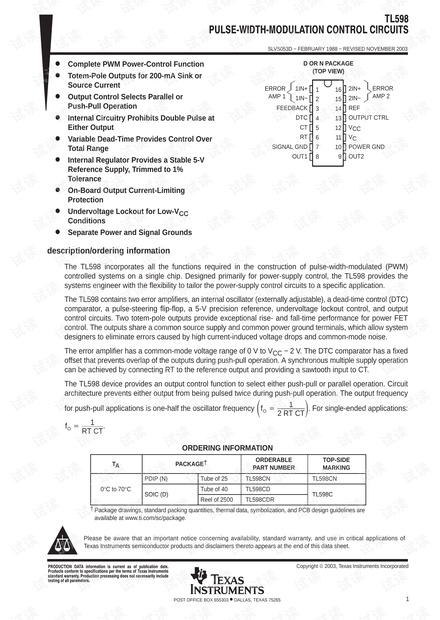
1IN+
1IN−
FEEDBACK
DTC
CT
RT
SIGNAL GND
OUT1
2IN+
2IN−
REF
OUTPUT CTRL
V
CC
V
C
POWER GND
OUT2
D OR N PACKAGE
(TOP VIEW)
ERROR
AMP 1
ERROR
AMP 2


剩余14页未读,继续阅读


评论0
最新资源