没有合适的资源?快使用搜索试试~ 我知道了~
TI-TL441.pdf
需积分: 5 0 下载量 156 浏览量
2022-11-26
21:48:22
上传
评论 4
收藏 989KB PDF 举报
温馨提示
试读
21页
TI-TL441.pdf
资源推荐
资源详情
资源评论
TL441
LOGARITHMIC AMPLIFIER
SLVS328 – OCTOBER 2000
1
POST OFFICE BOX 655303 • DALLAS, TEXAS 75265
D
Excellent Dynamic Range
D
Wide Bandwidth
D
Built-In Temperature Compensation
D
Log Linearity (30-dB Sections) ...1 dB Typ
D
Wide Input Voltage Range
description
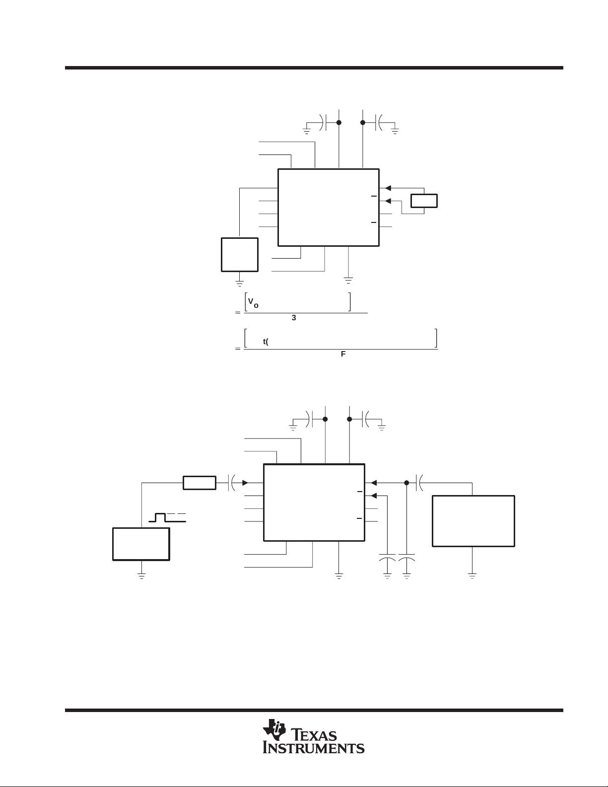
This amplifier circuit contains four 30-dB
logarithmic stages. Gain in each stage is such that
the output of each stage is proportional to the
logarithm of the input voltage over the 30-dB input
voltage range. Each half of the circuit contains two
of these 30-dB stages summed together in one
differential output that is proportional to the sum of the logarithms of the input voltages of the two stages. The
four stages may be interconnected to obtain a theoretical input voltage range of 120-dB. In practice, this permits
the input voltage range typically to be greater than 80-dB with log linearity of ± 0.5-dB (see application data).
Bandwidth is from dc to 40 MHz.
This circuit is useful in data compression and analog compensation. This logarithmic amplifier is used in log IF
circuitry as well as video and log amplifiers.
The TL441 is characterized for operation over 0°C to 70°C.
Copyright 2000, Texas Instruments Incorporated
PRODUCTION DATA information is current as of publication date.
Products conform to specifications per the terms of Texas Instruments
standard warranty. Production processing does not necessarily include
testing of all parameters.
1
2
3
4
5
6
7
8
16
15
14
13
12
11
10
9
C
A2
V
CC
–
C
A2′
A1
Y
Y
A2
V
CC
+
NC
C
B2
C
B2′
GND
B1
Z
Z
B2
N PACKAGE
(TOP VIEW)
NC — No internal connection
Please be aware that an important notice concerning availability, standard warranty, and use in critical applications of
Texas Instruments semiconductor products and disclaimers thereto appears at the end of this data sheet.
TL441
LOGARITHMIC AMPLIFIER
SLVS328 – OCTOBER 2000
2
POST OFFICE BOX 655303 • DALLAS, TEXAS 75265
functional logic diagram (one half)
–15 dB
–15 dB
Log
Log
Log
Log
Σ
Y (Z)
Y
(Z)
A1
(B1)
C
A2
(C
B2
)
C
A2′
(C
B2′
)
A2
(B2)
Y ∝ log A1 + log A2; Z ∝ log B1 + log B2 where: A1, A2, B1, and B2 are in dBV, 0 dBV = 1 V.
C
A2
, C
A2′
, C
B2
, and C
B2′
are detector compensation inputs.
schematic
V
CC
+
Y
Y
A2
A1
C
A2′
C
A2
V
CC –
8
6
5
7
4
3
1
2
10
11
9
12
13
14
15
Z
Z
B2
B1
GND
C
B2′
C
B2
TL441
LOGARITHMIC AMPLIFIER
SLVS328 – OCTOBER 2000
3
POST OFFICE BOX 655303 • DALLAS, TEXAS 75265
absolute maximum ratings over operating free-air temperature range (unless otherwise noted)
†
Supply voltages (see Note 1): V
CC+
8 V. . . . . . . . . . . . . . . . . . . . . . . . . . . . . . . . . . . . . . . . . . . . . . . . . . . . . . . . . . .
V
CC
–
–8 V. . . . . . . . . . . . . . . . . . . . . . . . . . . . . . . . . . . . . . . . . . . . . . . . . . . . . . . . .
Input voltage (see Note 1) 6 V. . . . . . . . . . . . . . . . . . . . . . . . . . . . . . . . . . . . . . . . . . . . . . . . . . . . . . . . . . . . . . . . . . . .
Output sink current (any one output) 30 mA. . . . . . . . . . . . . . . . . . . . . . . . . . . . . . . . . . . . . . . . . . . . . . . . . . . . . . . .
Package thermal impedance, θ
JA
(see Notes 2 and 3) 67°C/W. . . . . . . . . . . . . . . . . . . . . . . . . . . . . . . . . . . . . . .
Lead temperature 1,6 mm (1/16 inch) from case for 10 seconds 260°C. . . . . . . . . . . . . . . . . . . . . . . . . . . . . . .
Storage temperature range, T
stg
–65°C to 150°C. . . . . . . . . . . . . . . . . . . . . . . . . . . . . . . . . . . . . . . . . . . . . . . . . . .
†
Stresses beyond those listed under “absolute maximum ratings” may cause permanent damage to the device. These are stress ratings only, and
functional operation of the device at these or any other conditions beyond those indicated under “recommended operating conditions” is not
implied. Exposure to absolute-maximum-rated conditions for extended periods may affect device reliability.
NOTES: 1. All voltages, except differential out voltages, are with respect to network ground terminal.
2. Maximum power dissipation is a function of T
J
(max),
θ
JA
, and T
A
. The maximum allowable power dissipation at any allowable
ambient temperature is P
D
= (T
J
(max) – T
A
)/
θ
JA
. Operating at the absolute maximum T
J
of 150°C can affect reliability.
3. The package thermal impedance is calculated in accordance with JESD 51-7.
recommended operating conditions
MIN MAX UNIT
Peak-to-peak input voltage for each 30-dB stage 0.01 1 V
Operating free-air temperature, T
A
0 70 °C
electrical characteristics, V
CC±
= ±6 V, T
A
= 25°C
PARAMETER
TEST
FIGURE
MIN TYP MAX UNIT
Differential output offset voltage 1 ±40 mV
Quiescent output voltage 2 5.45 5.6 5.85 V
DC scale factor (differential output), each 3-dB stage, – 35 dBV to – 5 dBV 3 6 8 12 mV/dB
AC scale factor (differential output) 8 mV/dB
DC error at – 20 dBV (midpoint of – 35 dBV to – 5 dBV range) 3 1 dB
Input impedance 500 Ω
Output impedance 200 Ω
Rise time, 10% to 90% points, C
L
= 24 pF 4 20 30 ns
Supply current from V
CC+
2 14.5 18.5 23 mA
Supply current from V
CC
–
2 – 6 – 8.5 – 10.5 mA
Power dissipation 2 123 162 201 mW
TL441
LOGARITHMIC AMPLIFIER
SLVS328 – OCTOBER 2000
4
POST OFFICE BOX 655303 • DALLAS, TEXAS 75265
PARAMETER MEASUREMENT INFORMATION
Figure 1
V
CC+
V
CC–
C
A2
C
A2′
V
CC
+
V
CC
–
Y
Y
Z
Z
DVM
C
B2
C
B2′
GND
A1
A2
B1
B2
Figure 2
C
A2
C
A2′
V
CC+
V
CC–
Y
Y
Z
Z
C
B2
C
B2′
GND
A1
A2
B1
B2
V
CC+
V
CC–
I
CC
+
I
CC –
V
O
P
D
= V
CC+
• I
CC+
+ V
CC–
• I
CC–
TL441
LOGARITHMIC AMPLIFIER
SLVS328 – OCTOBER 2000
5
POST OFFICE BOX 655303 • DALLAS, TEXAS 75265
PARAMETER MEASUREMENT INFORMATION
C
A2
C
A2′
V
CC+
V
CC–
Y
Y
Z
Z
C
B2
GND
A1
A2
B1
B2
DVM
18 mV
100 mV
560 mV
DC
Power
Supply
V
CC+
V
CC–
Scale Factor
+
ƪ
V
out(560 mV)
–V
out(18mV)
ƫ
mV
30 dBV
Error
+
ƪ
Vout(100 mV)
–0.5 V
out(560 mV)
–0.5 V
out(18 mV)
ƫ
Scale Factor
C
B2′
Figure 3
C
A2
C
A2′
V
CC+
V
CC–
Y
Y
Z
Z
C
B2
C
B2′
GND
A1
A2
B1
B2
V
CC+
V
CC–
1000 pFC
I
C
L
C
L
100
mV
0
mV
Atten
Pulse
Generator
50
Ω
Tektronix
Sampling
Scope
With
Digital
Readout
or
Equivalent
NOTES: A. The input pulse has the following characteristics: t
w
= 200 ns, t
r
≤ 2 ns, t
f
≤ 2 ns, PRR ≤ 10 MHz.
B. Capacitor C
I
consists of three capacitors in parallel: 1 µF, 0.1 µF, and 0.01 µF.
C. C
L
includes probe and jig capacitance.
Figure 4
剩余20页未读,继续阅读
资源评论
不觉明了
- 粉丝: 3199
- 资源: 5526
上传资源 快速赚钱
- 我的内容管理 展开
- 我的资源 快来上传第一个资源
- 我的收益 登录查看自己的收益
- 我的积分 登录查看自己的积分
- 我的C币 登录后查看C币余额
- 我的收藏
- 我的下载
- 下载帮助
安全验证
文档复制为VIP权益,开通VIP直接复制
信息提交成功