没有合适的资源?快使用搜索试试~ 我知道了~
TI-TL026.pdf
需积分: 5 0 下载量 112 浏览量
2022-11-26
23:55:44
上传
评论 4
收藏 1.08MB PDF 举报
温馨提示
![preview](https://dl-preview.csdnimg.cn/87173602/0001-b0457d7ce82d7f9e47f61800745392a0_thumbnail.jpeg)
![preview-icon](https://csdnimg.cn/release/downloadcmsfe/public/img/scale.ab9e0183.png)
试读
19页
TI-TL026.pdf
资源推荐
资源详情
资源评论
![](https://csdnimg.cn/release/download_crawler_static/87173602/bg1.jpg)
TL026C
DIFFERENTIAL HIGH-FREQUENCY AMPLIFIER WITH AGC
SLFS007A – JUNE 1985 – REVISED JULY 1990
1
POST OFFICE BOX 655303 • DALLAS, TEXAS 75265
D
Low Output Common-Mode Sensitivity to
AGC Voltages
D
Input and Output Impedances Independent
of AGC Voltage
D
Peak Gain . . . 38 dB Typ
D
Wide AGC Range . . . 50 dB Typ
D
3-dB Bandwidth . . . 50 MHz
D
Other Characteristics Similar to NE592 and
uA733
description
This device is a monolithic two-stage high-
frequency amplifier with differential inputs and
outputs.
Internal feedback provides wide bandwidth, low phase distortion, and excellent gain stability. Variable gain
based on signal summation provides large AGC control over a wide bandwidth with low harmonic distortion.
Emitter-follower outputs enable the device to drive capacitive loads. All stages are current-source biased to
obtain high common-mode and supply-voltage rejection ratios. The gain may be electronically attenuated by
applying a control voltage to the AGC pin. No external compensation components are required.
This device is particularly useful in TV and radio IF and RF AGC circuits, as well as magnetic-tape and disk-file
systems where AGC is needed. Other applications include video and pulse amplifiers where a large AGC range,
wide bandwidth, low phase shift, and excellent gain stability are required.
The TL026C is characterized for operation from 0°C to 70°C.
absolute maximum ratings over operating free-air temperature range (unless otherwise noted)
†
Supply voltage, V
CC+
(see Note 1) 8 V. . . . . . . . . . . . . . . . . . . . . . . . . . . . . . . . . . . . . . . . . . . . . . . . . . . . . . . . . . . .
Supply voltage, V
CC–
(see Note 1) – 8 V. . . . . . . . . . . . . . . . . . . . . . . . . . . . . . . . . . . . . . . . . . . . . . . . . . . . . . . . . .
Differential input voltage ±5 V. . . . . . . . . . . . . . . . . . . . . . . . . . . . . . . . . . . . . . . . . . . . . . . . . . . . . . . . . . . . . . . . . . . .
Common-mode input voltage ±6 V. . . . . . . . . . . . . . . . . . . . . . . . . . . . . . . . . . . . . . . . . . . . . . . . . . . . . . . . . . . . . . . .
Output current ±10 mA. . . . . . . . . . . . . . . . . . . . . . . . . . . . . . . . . . . . . . . . . . . . . . . . . . . . . . . . . . . . . . . . . . . . . . . . . .
Continuous total dissipation See Dissipation Rating Table. . . . . . . . . . . . . . . . . . . . . . . . . . . . . . . . . . . . . . . . . . .
Operating free-air temperature range 0°C to 70°C. . . . . . . . . . . . . . . . . . . . . . . . . . . . . . . . . . . . . . . . . . . . . . . . . .
Storage temperature range – 65°C to 150°C. . . . . . . . . . . . . . . . . . . . . . . . . . . . . . . . . . . . . . . . . . . . . . . . . . . . . . .
Lead temperature range 1,6 mm (1/16 inch) from case for 10 seconds 260°C. . . . . . . . . . . . . . . . . . . . . . . . . .
†
Stresses beyond those listed under absolute maximum ratings may cause permanent damage to the device. This is a stress rating only, and
functional operation of the device at these or any other conditions beyond those indicated in the recommended operating conditions section of
this specification is not implied. Exposure to absolute-maximum-rated conditions for extended periods may affect device reliability.
NOTE 1: All voltages are with respect to the midpoint of V
CC+
and V
CC–
except differential input and output voltages.
DISSIPATION RATING TABLE
PACKAGE
T
A
≤ 25°C
POWER RATING
OPERATING FACTOR
ABOVE T
A
= 25°C
T
A
= 70°C
POWER RATING
D 725 mW 5.8 mW/°C 464 mW
P 1000 mW 8.0 mW/°C 640 mW
Copyright 1990, Texas Instruments Incorporated
PRODUCTION DATA information is current as of publication date.
Products conform to specifications per the terms of Texas Instruments
standard warranty. Production processing does not necessarily include
testing of all parameters.
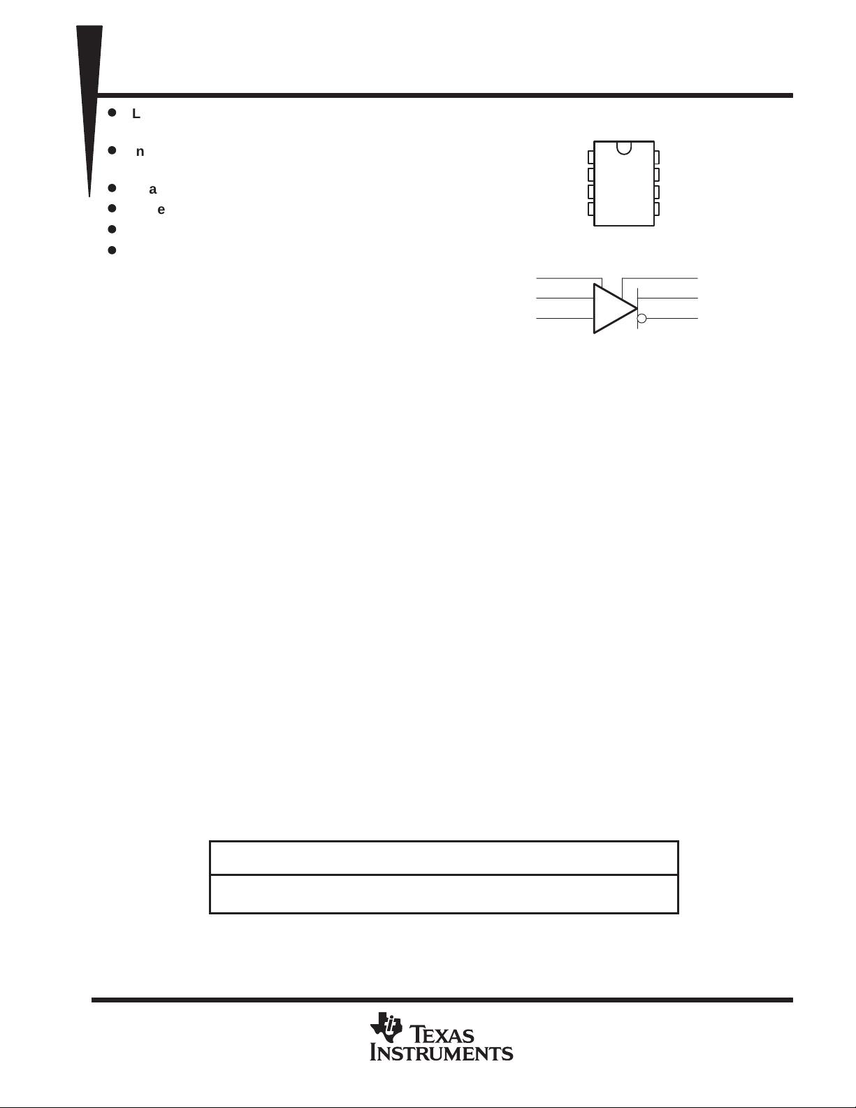
IN–
REF OUT
V
CC
+
OUT–
1
2
3
4
8
7
6
5
IN+
AGC
V
CC
OUT+
D OR P PACKAGE
(TOP VIEW)
symbol
+
–
AGC
IN +
IN –
7
4
5
2
1
8
REF OUT
OUT+
OUT–
![](https://csdnimg.cn/release/download_crawler_static/87173602/bg2.jpg)
TL026C
DIFFERENTIAL HIGH-FREQUENCY AMPLIFIER WITH AGC
SLFS007A – JUNE 1985 – REVISED JULY 1990
2
POST OFFICE BOX 655303 • DALLAS, TEXAS 75265
recommended operating conditions
MIN NOM MAX UNIT
Supply voltage, V
CC
+
3 6 8 V
Supply voltage, V
CC
–
– 3 – 6 – 8 V
Operating free-air temperature range, T
A
0 70 °C
electrical characteristics at 25°C operating free-air temperature, V
CC+
= ±6 V, V
AGC
= 0, REF OUT pin
open (unless otherwise specified)
PARAMETER FIGURE TEST CONDITIONS MIN TYP MAX UNIT
A
VD
Large-signal differential voltage
amplification
1 V
O(PP)
= 3 V, R
L
= 2 kΩ 65 85 105 V/V
∆A
VD
Change in voltage amplification 1
V
IPP
= 28.5 mV, R
L
= 2 kΩ,
V
AGC
– V
ref
= ±180 mV
– 50 dB
V
ref
Voltage at REF OUT I
ref
= – 1 mA to 100 µA 1.3 1.5 V
BW Bandwidth (–3 dB) 2
V
O(PP)
= 1 V,
V
AGC
– V
ref
= ±180 mV
50 MHz
I
IO
Input offset current 0.4 5 µA
I
IB
Input bias current 10 30 µA
V
ICR
Common-mode input voltage range 3 ±1 V
V
OC
Common-mode output voltage 1 R
L
= ∞ 3.25 3.75 4.25 V
∆V
OC
Change in common-mode output voltage 1 V
AGC
= 0 to 2 V, R
L
= ∞ 300 mV
V
OO
Output offset voltage 1 V
ID
= 0, R
L
= ∞ 0.75 V
V
O(PP)
Maximum peak-to-peak output voltage
swing
1 R
L
= 2 kΩ 3 4 V
r
i
Input resistance at AGC, IN+, or IN – 10 30 kΩ
r
o
Output resistance 20 Ω
CMRR
Common mode rejection ratio
3
V
IC
= ±1 V, f = 100 kHz 60 86
dB
CMRR
Common
-
mode
rejection
ratio
3
V
IC
= ±1 V, f = 5 mHz 60
dB
k
SVR
Supply voltage rejection ratio
(∆V
CC
/ ∆V
IO
)
4
∆V
CC
+
= ± 0.5 V,
∆V
CC
–
= ± 0.5 V
50 70 dB
V
n
Broadband equivalent noise voltage 4 BW = 1 kHz to 10 MHz 12 µV
t
pd
Propagation delay time 2 ∆V
O
= 1 V 6 10 ns
t
r
Rise time 2 ∆V
O
= 1 V 4.5 12 ns
I
sink(max)
Maximum output sink current V
ID
= 1 V, V
O
= 3 V 3 4 mA
I
CC
Supply current No load, No signal 22 27 mA
![](https://csdnimg.cn/release/download_crawler_static/87173602/bg3.jpg)
TL026C
DIFFERENTIAL HIGH-FREQUENCY AMPLIFIER WITH AGC
SLFS007A – JUNE 1985 – REVISED JULY 1990
3
POST OFFICE BOX 655303 • DALLAS, TEXAS 75265
electrical characteristics over recommended operating free-air temperature range, V
CC
±
= ±6 V,
V
AGC
= 0, REF OUT pin open (unless otherwise specified)
PARAMETER FIGURE TEST CONDITIONS MIN TYP MAX UNIT
A
VD
Large-signal differential voltage amplification 1 V
O(PP)
= 3 V, R
L
= 2 kΩ 55 115 V/V
I
IO
Input offset current 6 µA
I
IB
Input bias current 40 µA
V
ICR
Common-mode input voltage range 3 ±1 V
V
OO
Output offset voltage 1 V
ID
= 0, R
L
= ∞ 1.5 V
V
O(PP)
Maximum peak-to-peak output voltage swing 1 R
L
= 2 kΩ 2.8 V
r
i
Input resistance at AGC, IN+, or IN – 8 kΩ
CMRR Common-mode rejection ratio 3 V
IC
= ±1 V, f = 100 kHz 50 dB
k
SVR
Supply voltage rejection ratio
(∆V
CC
/ ∆V
IO
)
4
∆V
CC
+
= ± 0.5 V,
∆V
CC
–
= ± 0.5 V
50 dB
I
sink(max)
Maximum output sink current V
ID
= 1 V, V
O
= 3 V 2.8 4 mA
I
CC
Supply current 1 No load, No signal 30 mA
PARAMETER MEASUREMENT INFORMATION
IN +
IN –
AGC
OUT +
OUT –
REF OUT
R
L
50 Ω 50 Ω
V
OC
+
V
O
)
)
V
O
*
2
+
–
V
AGC
V
ref
V
ID
V
OD
Figure 1. Test Circuit
1 kΩ1 kΩ
V
O
+
V
O
–
50 Ω 50 Ω
+
–
V
ID
0.2 µF
0.2 µF
Figure 2. Test Circuit
1 kΩ1 kΩ
V
O
+
V
O
–
50 Ω
50 Ω
+
–
0.2 µF
0.2 µF
V
IC
Figure 3. Test Circuit
R
L
= 2 kΩ
+
–
V
OD
Figure 4. Test Circuit
![](https://csdnimg.cn/release/download_crawler_static/87173602/bg4.jpg)
TL026C
DIFFERENTIAL HIGH-FREQUENCY AMPLIFIER WITH AGC
SLFS007A – JUNE 1985 – REVISED JULY 1990
4
POST OFFICE BOX 655303 • DALLAS, TEXAS 75265
TYPICAL CHARACTERISTICS
Figure 5
– 200 – 100 0 100 200
A
DIFFERENTIAL VOLTAGE AMPLIFICATION
vs
DIFFERENTIAL GAIN-CONTROL VOLTAGE
VD
V
AGC
– V
ref
– Differential Gain-Control Voltage – mV
100
90
80
70
60
50
40
30
20
10
0
V
CC
+
= 6 V
V
CC
–
= – 6 V
T
A
= 0°C
T
A
= 70°C
T
A
= 25°C
— Differential Voltage Amplification — V/ V
剩余18页未读,继续阅读
资源评论
![avatar-default](https://csdnimg.cn/release/downloadcmsfe/public/img/lazyLogo2.1882d7f4.png)
![avatar](https://profile-avatar.csdnimg.cn/107303f5121d47e49d12d0a9ae68af10_weixin_54787054.jpg!1)
不觉明了
- 粉丝: 3226
- 资源: 5611
上传资源 快速赚钱
我的内容管理 展开
我的资源 快来上传第一个资源
我的收益
登录查看自己的收益我的积分 登录查看自己的积分
我的C币 登录后查看C币余额
我的收藏
我的下载
下载帮助
![voice](https://csdnimg.cn/release/downloadcmsfe/public/img/voice.245cc511.png)
![center-task](https://csdnimg.cn/release/downloadcmsfe/public/img/center-task.c2eda91a.png)
安全验证
文档复制为VIP权益,开通VIP直接复制
![dialog-icon](https://csdnimg.cn/release/downloadcmsfe/public/img/green-success.6a4acb44.png)