

Product
Folder
Sample &
Buy
Technical
Documents
Tools &
Software
Support &
Community
TLK111
SLLSEF8C –AUGUST 2013–REVISED NOVEMBER 2014
TLK111 PHYTER
®
Industrial Temperature 10/100Mbs Ethernet Physical Layer Transceiver
1 Introduction
1.1 Features
1
• Fully Pin Compatible with the TLK110 Device • Error-Free 100Base-T Operation up to 150 Meters
Under Typical Conditions
• Low Power Consumption:
• Error-Free 10Base-T Operation up to 300 Meters
– Single Supply: <205mW PHY, 275mW with
Under Typical Conditions
Center Tap (Typical)
• Serial Management Interface
– Dual Supplies: <126mW PHY, 200mW with
Center Tap (Typical) • IEEE 802.3u ENDEC, 10Base-T
Transceivers and Filters
• Programmable Power Back Off to reduce PHY
power up to 20% in systems with shorter cables • IEEE 802.3u PCS, 100Base-TX Transceivers
• IEEE 1588 SFD indication enables time stamping • IEEE 1149.1 JTAG
by a controller or processor
• Integrated ANSI X3.263 Compliant TP-PMD
• Low deterministic latency supports IEEE1588 Physical Sublayer with Adaptive Equalization and
implementation Baseline Wander Compensation
• Cable Diagnostics • Programmable LED Support Link, 10/100Mbs
Mode, Activity, and Collision Detect
• Programmable Fast Link Down Modes, <10µs
reaction time • 10/100Mbs Packet BIST (Built in Self Test)
• Variable I/O voltage range: 1.8V to 3.3V • HBM ESD protection on RD± and TD± of 16kV
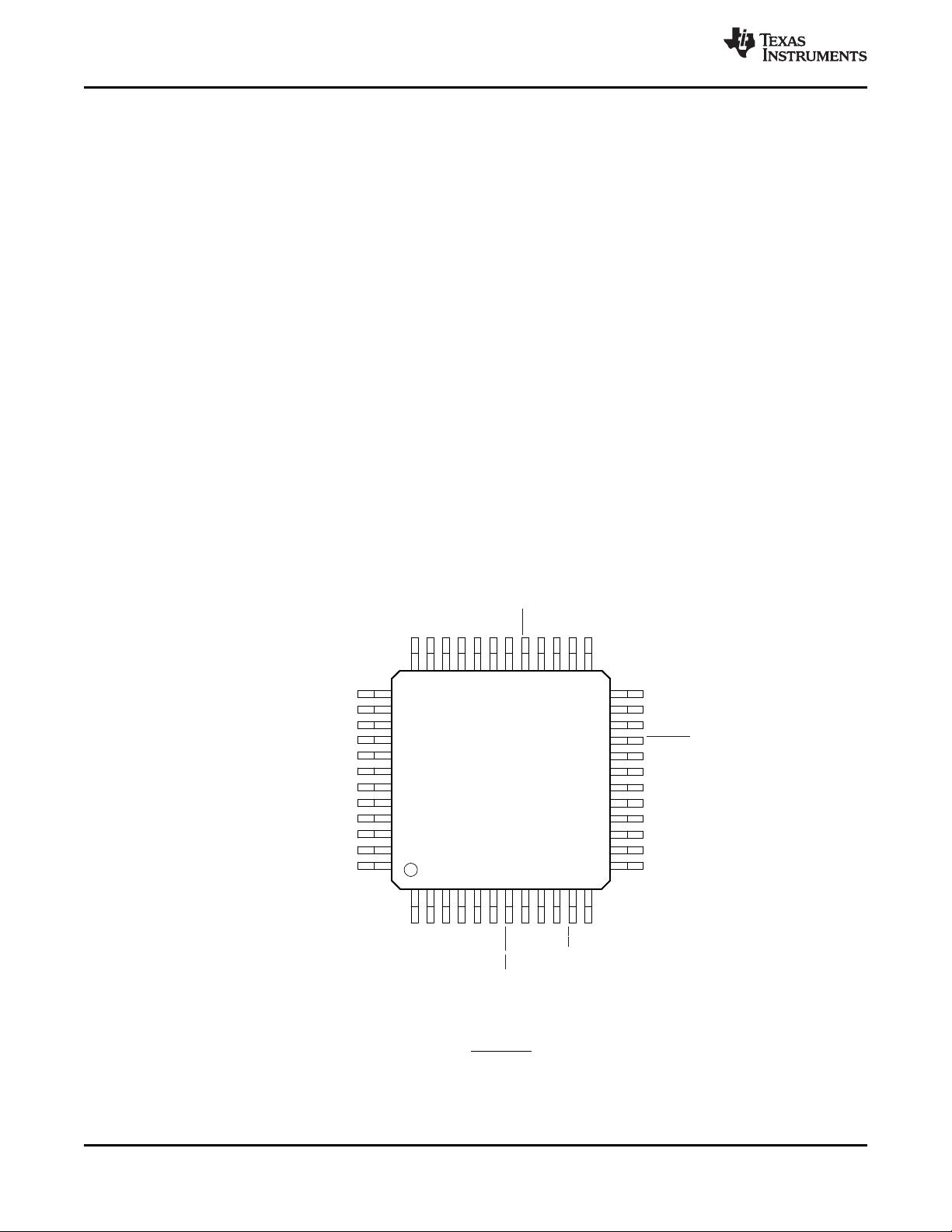
• 3.3-V MAC Interface • 48-pin LQFP Package (7mm) × (7mm)
• Fixed TX Clock to XI, with programmable phase
shift
• Auto-MDIX for 10/100Mbs
• Energy Detection Mode
• 25 MHz Clock Out
• MII and RMII Capabilities
• IEEE 802.3u MII
• IEEE 802.3u Auto-Negotiation and Parallel
Detection
1.2 Applications
• Industrial Networks and Factory Automation • Motor and Motion Control
• Real Time Industrial Ethernet Applications such as • General Embedded Applications
EtherCAT
®
, Ethernet/IP™, ProfiNET
®
, and
SERCOSIII
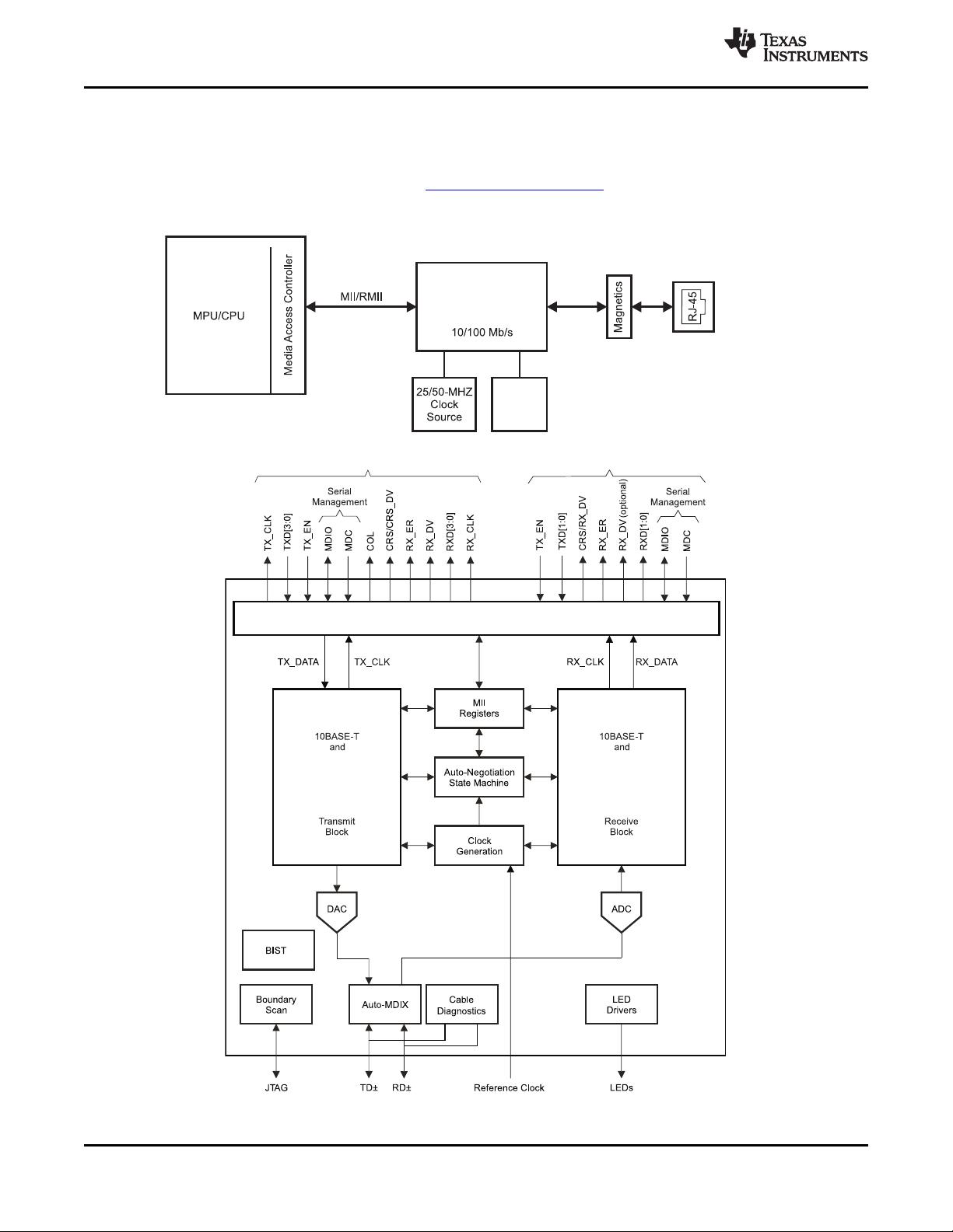
1.3 Description
The TLK111 is a single-port Ethernet PHY for 10Base-T and 100Base TX signaling. This device integrates
all the physical-layer functions needed to transmit and receive data on standard twisted-pair cables.
The TLK111 supports the standard Media Independent Interface (MII) and Reduced Media Independent
Interface (RMII) for direct connection to a Media Access Controller (MAC).
The TLK111 is designed for power-supply flexibility, and can operate with a single 3.3V power supply or
with combinations of 3.3V and 1.55V power supplies for reduced power operation.
The TLK111 uses mixed-signal processing to perform equalization, data recovery, and error correction to
achieve robust operation over CAT 5 twisted-pair wiring. This device not only meets the requirements of
IEEE 802.3, but maintains high margins in terms of cross-talk and alien noise.
1
An IMPORTANT NOTICE at the end of this data sheet addresses availability, warranty, changes, use in safety-critical applications,
intellectual property matters and other important disclaimers. PRODUCTION DATA.


剩余104页未读,继续阅读
资源评论


不觉明了
- 粉丝: 8292
- 资源: 5764


最新资源
- python操作arxml.txt
- python操作abaqus.txt
- python操作excel图片.txt
- python操作gitlab.txt
- python操作excel导出图片.txt
- python操作mysql教程pdf.txt
- python操作pdf和ppt.txt
- python操作pdfminer.txt
- python操作pdf文件.txt
- python操作pdf获取文本.txt
- python操作table标签.txt
- python操作ts音频流.txt
- python操作tsc打印机打印.txt
- python操作txt删除行.txt
- python操作word插入图片.txt
- python操作xml导入什么库.txt
资源上传下载、课程学习等过程中有任何疑问或建议,欢迎提出宝贵意见哦~我们会及时处理!
点击此处反馈


