TI-TLK100.pdf
需积分: 5 173 浏览量
2022-12-16
21:38:29
上传
评论 3
收藏 1.35MB PDF 举报


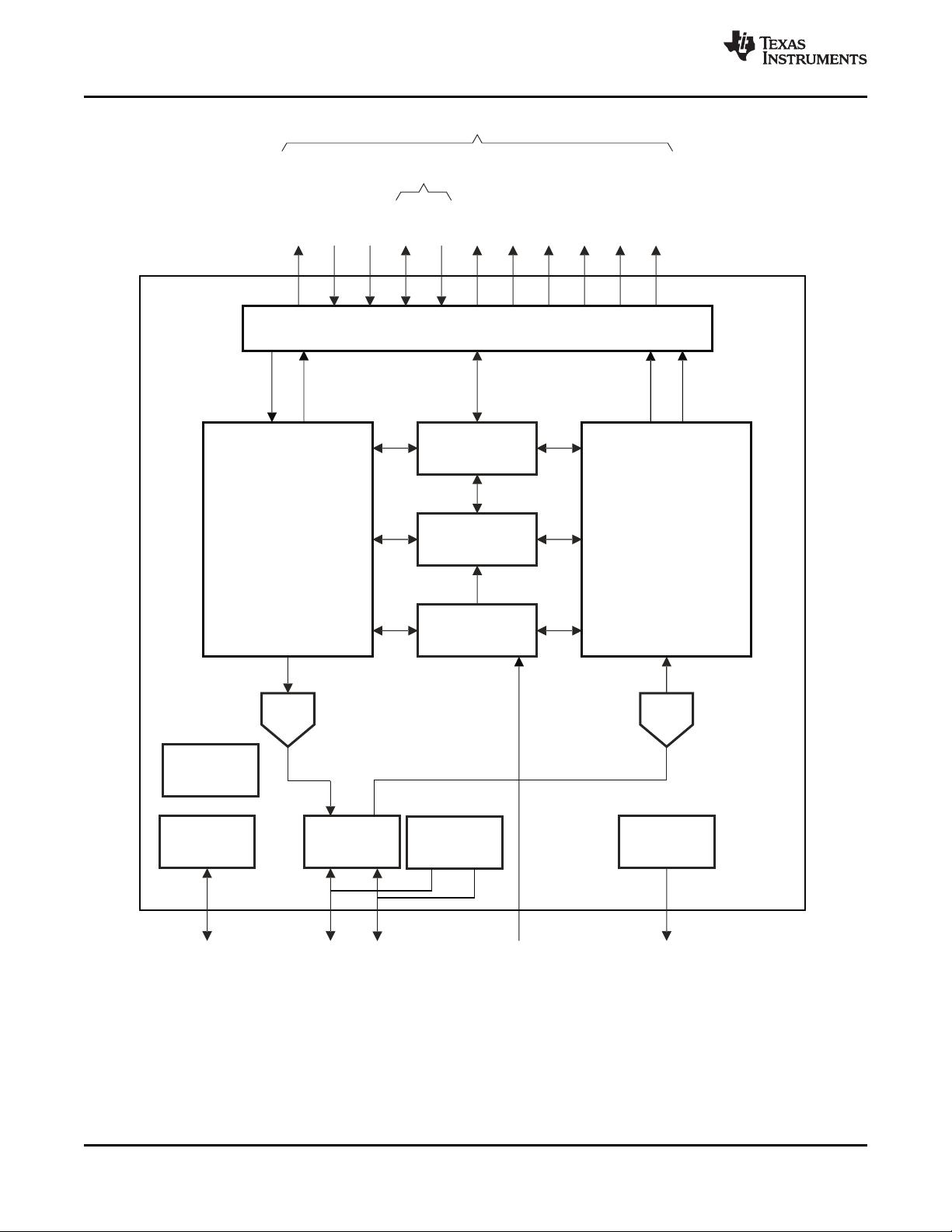
Magnetics
MPU/CPU
Media AccessController
MII
10/100Mb/s
TLK100
25-MHz
Clock
Source
Status
LEDs
RJ-45
10BASE-T
or
100BASE-TX
B0312-01
TLK100
www.ti.com
SLLS931B–AUGUST 2009–REVISED DECEMBER 2009
Industrial Temp, Single Port 10/100 Mb/s Ethernet Physical Layer Transceiver
Check for Samples: TLK100
1 Introduction
1.1 Features
1
• Temperature From –40°C to 85°C • Bus I/O Protection - ±16kV JEDEC HBM
• Low Power Consumption, < 200mW Typical • IEEE 802.3u PCS, 100BASE-TX Transceivers
• Cable Diagnostics • Enables IEEE1588 Time-Stamping
• Error-Free Operation up to 200 Meters Under • IEEE 1149.1 JTAG
Typical Conditions
• Integrated ANSI X3.263 Compliant TP-PMD
• 3.3V MAC Interface Physical Sublayer with Adaptive Equalization
and Baseline Wander Compensation
• Auto-MDIX for 10/100 Mb/s
• Programmable LED Support Link, 10/100 Mb/s
• Energy Detection Mode
Mode, Activity, and Collision Detect
• 25 MHz Clock Out
• 10/100 Mb/s Packet BIST (Built in Self Test)
• MII Serial Management Interface (MDC and
• 48-pin TQFP Package (7mm) × (7mm)
MDIO)
• IEEE 802.3u MII
1.2 Applications
• IEEE 802.3u Auto-Negotiation and Parallel
Detection
• Industrial Controls and Factory Automation
• IEEE 802.3u ENDEC, 10BASE-T
• General Embedded Applications
Transceivers and Filters
1.3 General Description
The TLK100 is a single-port Ethernet PHY for 10BaseT and 100Base TX signaling. It integrates all the
physical-layer functions needed to transmit and receive data on standard twisted-pair cables. This device
supports the standard Media Independent Interface (MII) for direct connection to a Media Access
Controller (MAC).
The TLK100 is designed for power-supply flexibility, and can operate with a single 3.3V power supply or
with combinations of 3.3V, 1.8V, and 1.1V power supplies for reduced power operation.
The TLK100 uses mixed-signal processing to perform equalization, data recovery, and error correction to
achieve robust operation over CAT 5 twisted-pair wiring. It not only meets the requirements of IEEE 802.3,
but maintains high margins in terms of cross-talk and alien noise.
1.4 System Diagram
1
Please be aware that an important notice concerning availability, standard warranty, and use in critical applications of Texas
Instruments semiconductor products and disclaimers thereto appears at the end of this data sheet.
PRODUCTION DATA information is current as of publication date.
Copyright © 2009, Texas Instruments Incorporated
Products conform to specifications per the terms of the Texas
Instruments standard warranty. Production processing does not
necessarily include testing of all parameters.


剩余89页未读,继续阅读
资源评论


